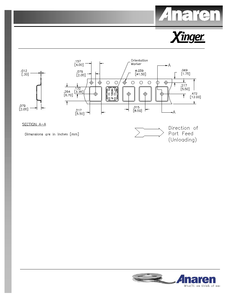
Available on Tape
and Reel For Pick and
Place Manufacturing.
USA/Canada:
Toll Free:
Europe
:
(315) 432-8909
(800) 544-2414
+44 2392-232392
Model JP510
Rev A
Pico Xinger
10dB Directional Coupler
Description
The JP510 Pico Xinger is a low profile, miniature 10dB directional coupler in
an easy to use surface mount package designed for UMTS and WCDMA
applications. The JP510 is for power and frequency detection as well as
power injection. The JP510 is an ideal solution for the ever-increasing
demands of the wireless industry for smaller printed circuit boards and high
performance. Parts have been subjected to rigorous qualification testing
and units are 100% tested. They are manufactured using materials with x
and y thermal expansion coefficients compatible with common substrates.
ELECTRICAL
SPECIFICATIONS**
Frequency
Mean
Coupling
Insertion
Loss
VSWR
Freq.
Sensitivity
GHz
dB
dB Max
Max : 1
dB Max
2.0 2.3
10 ± 0.75
0.25
1.22
± 0.2
Directivity
Power
Handling
JC
Operating
Temp.
dB Min
Ave CW Watts
ºC / Watt
ºC
Features:
· 2.0 2.3 GHz
· UMTS and WCDMA
· Very Low Loss
· High Directivity
· Surface Mountable
· Tape and Reel
· New Pico-Package
· 100% Tested
20
20
44
-55 to +85
**Specification based on performance of unit properly installed on microstrip printed circuit
boards with 50
nominal impedance. Specifications subject to change without notice.
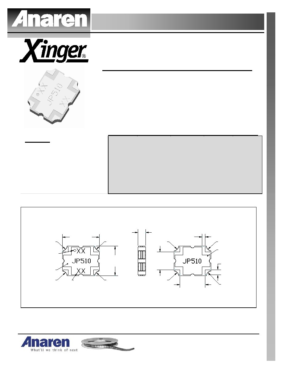
JP510 Rev A Mechanical Outline
Dimensions are in Inches [Millimeters]
.250
±.010
[6.35
±0.25
]
.200
±.010
[5.08
±0.25
]
.051
±.005
[1.29
±0.13
]
Top View (Near-side)
Side View
Bottom View (Far-side)
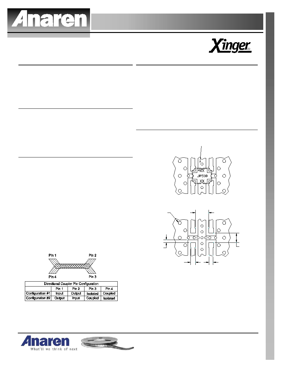
Pin 4
Pin 1
Pin 2
Pin 3
Pin 1
Pin 4
Pin 3
Pin 2
4X .020
±.004
[0.51
±0.10
]
GND
Orientation
Marker Denotes
Pin Location
4X .034
±.004
SQ
[0.86
±0.10
]
Tolerances are Non-Cumulative
.170
±.004
[4.32
±0.10
]
.120
±.004
[3.05
±0.10
]
GND
Denotes
Array number
USA/Canada:
Toll Free:
Europe:
(315) 432-8909
(800) 544-2414
+44 2392-232392
Available on Tape and
Reel For Pick and Place
Manufacturing.
Model JP510
Rev A
Typical Performance: 1.7 GHz. 2.6 GHz.
Coupling JP510
-11.5
-11.0
-10.5
-10.0
-9.5
1700
1900
2100
2300
2500
Frequency (MHz)
C
oup
l
i
n
g (
d
B
)
Return Loss JP510
-50
-40
-30
-20
-10
0
1700
1900
2100
2300
2500
Frequency (MHz)
R
e
t
u
r
n
L
o
ss (
d
B
)
Directivity JP510
-50
-40
-30
-20
-10
0
1700
1900
2100
2300
2500
Frequency (MHz)
D
i
r
e
c
t
iv
it
y
(
d
B
)
Transmission Loss JP510
-1.00
-0.80
-0.60
-0.40
-0.20
0.00
1700
1900
2100
2300
2500
Frequency (MHz)
T
r
a
n
sm
i
ssi
o
n
L
o
ss (
d
B
)
COUPLING
Choice of a coupling value in an application normally
depends on the power level of the main (sampled) line.
For example, if the coupler is being used to monitor main
line power, the coupling value is selected to provide
sufficient power to the monitoring device and yet
minimize system loss. Note that any coupler reduces
power flowing in the main line by the amount coupled off;
a 10dB coupler reduces main line power by 1 dB (10%)
where a 20dB coupler reduces it by only 0.044dB (1%).
Anaren uses mean coupling and frequency sensitivity
with the coupling specification. The mean coupling value
is arrived at by periodically sampling the coupling value
over the specified band and averaging the readings.
Frequency
sensitivity is the peak to peak variation in
coupling over the specified band.
VSWR & DIRECTIVITY
In directional couplers, directivity is specified in lieu of
isolation. Directivity is a measure of how well the coupled
power is isolated from reflections at the main line output
port. For example, open or short circuiting the output port
of a coupler with 20dB directivity would only affect the
coupled output power by 1% and only 0.1% for 30dB
directivity. High directivity is especially important if the
coupler is being used to measure the VSWR of a device
at its output port. In this application, accurate
measurements of forward and reverse power are
required.
In theory, VSWR and directivity characteristics of a
coupler are perfect; the input and output ports are
perfectly matched and no power is coupled to the isolated
port. In practice, factors associated with the design and
manufacturing processes limit VSWR and directivity. The
Available on Tape
and Reel For Pick and
Place Manufacturing.
USA/Canada:
Toll Free:
Europe
:
(315) 432-8909
(800) 544-2414
+44 2392-232392
Model JP510
Rev A
VSWR & DIRECTIVITY (CONTINUED)
internal meandering of the coupled lines and limitations
of building perfect 50
transitions at the input and
output ports of the device are the most significant
factors against perfect VSWR and directivity.
Typically, VSWR and directivity of 1.15:1 and 25 dB
respectively are achieved in practice.
INSERTION LOSS
Coupler insertion loss is defined as the log of the input
power divided by the sum of the power at the two
output ports. In practice, typical loss is approximately
0.20 dB. Specification limits are somewhat higher due
to imperfect test conditions; surface mount couplers
must be tested in test fixtures that negatively affect
results.
PIN CONFIGURATION
The JP510's have an orientation marker to denote
either pin 1 or pin 2. When the input port is identified,
the output, coupled and isolated ports are known
automatically. For example, if the input port for a
device was selected to be Pin 1, Pin 2 automatically
becomes the output port, Pin 4 becomes the coupled
port, and Pin 3 is the isolated port. Similarly, if Pin 2
was to be selected as the input port, the adjacent port
on the long side (Pin 1) is the output port, the adjacent
port on the short side (Pin 3) is the coupled port, and
the opposite port (Pin 4) is the isolated port. Either
port on the same side as the orientation marker can be
selected as the input port, as shown in the table, which
shows both pin configurations
.
The use of pin 1 or pin
2 as the input port ensures phase consistency as well
as maximum power handling.
MOUNTING
For Xinger surface mount couplers to operate optimally,
there must be 50
transmission lines leading to and from
all of the RF ports. To ensure proper electrical and
thermal performance, there must be a ground plane with
100% solder connection underneath the part. If either of
these two conditions is not satisfied, insertion loss,
coupling, VSWR and directivity may not meet published
specifications.
SUGGESTED FOOTPRINT
JP510 Rev A Mounting Footprint
Dimensions are in Inches [Millimeters]
To ensure proper electrical and thermal performance
there must be a ground plane with 100%
solder connection underneath the part
4X .063 SQ
[1.60]
4X .034
[0.86]
.170
[4.32]
.120
[3.05]
4X 50
Transmission
Line
Multiple
plated thru holes
to ground