 | ÐлекÑÑоннÑй компоненÑ: FB650 | СкаÑаÑÑ:  PDF PDF  ZIP ZIP |
Microsoft Word - FB650 Rev B.doc
Available on Tape
and Reel For Pick and
Place Manufacturing.
USA/Canada:
Toll Free:
Europe
:
(315) 432-8909
(800) 544-2414
+44 2392-232392
Model FB650
Rev. B
rit
Femto Balun
50 to 100 Balanced
Description
The FB650 is a low profile sub-miniature balanced to unbalanced transformer
designed for differential inputs and output locations on next generation wireless
chipsets in an easy to use surface mount package covering 802.11b. The FB650 is
ideal for high volume manufacturing and is higher performance than traditional
ceramic baluns. The FB650 has an unbalanced port impedance of 50
and a 50
balanced port impedance*. This transformation enables single ended signals to be
applied to differential ports on modern integrated chipsets. The output ports have
equal amplitude (-3dB) with 180 degree phase differential. The FB650 is available
on tape and reel for pick and place high volume manufacturing.
ELECTRICAL
SPECIFICATIONS**
Frequency
Unbalanced
Port
Impedance
Balanced
Port
Impedance*
Return
Loss
Insertion
Loss
GHz
Ohms
Ohms
dB min
dB max
2.4 2.5
50
100
17
0.55***
Amplitude
Balance
Phase
Balance
Power
Handling
JC
Operating
Temp.
dB
Degrees max
Watts
ºC / Watt
ºC
Features:
· 2.4 2.5 GHz
· 180° Transformer
· 50 Ohm to 2 x 50 Ohm
· Low Insertion Loss
· Medium Power
· No DC Decoupling Capacitors
Required
· Input to Output DC Isolation
· Surface Mountable
· Tape & Reel
· Convenient Package
0 ± 0.5
180 ± 5.0
4
28
-55 to +85
**Specification based on performance of unit properly installed on microstrip printed circuit
boards with 50
nominal impedance. Specifications subject to change without notice.
* 50
reference to ground
*** Insertion Loss stated at room temperature (0.6 dB Max at +85 ºC)
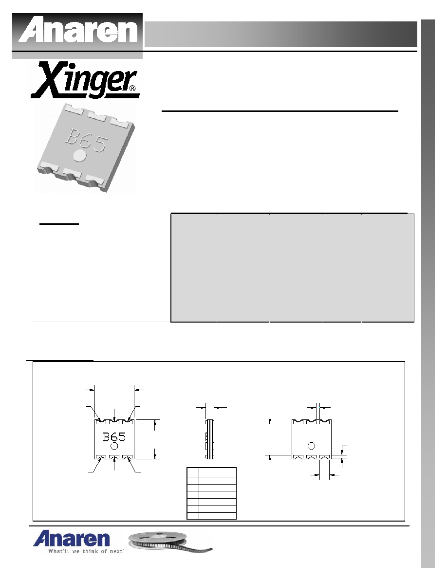
Outline Drawing
FB650 Rev B Mechanical Outline
Dimensions are in Inches [Millimeters]
Side View
Top View (Near-side)
Bottom View (Far-side)
.024
±.002
[0.61
±0.05
]
.120
±.005
[3.05
±0.13
]
.120
±.005
[3.05
±0.13
]
4
5
6
3
1
2
6X .030
±.004
[0.76
±0.10
]
4X .010
±.004
[0.25
±0.10
]
.095
±.004
[2.41
±0.10
]
6X .009
±.004
[0.23
±0.10
]
GND
In
GND
Out 2
GND
Out 1
Designation
5
4
2
1
6
3
Pin
Tolerances are Non-Cumulative
USA/Canada:
Toll Free:
Europe:
(315) 432-8909
(800) 544-2414
+44 2392-232392
Available on Tape and
Reel For Pick and Place
Manufacturing.
Model FB650
Rev. B
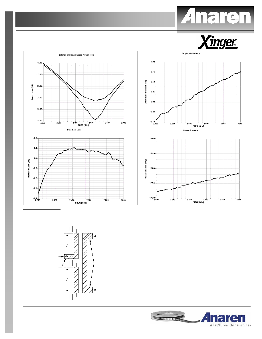
Typical Performance: 2.0 GHz. to 3.0 GHz.
Pin Configuration:
Balun Pin Configruation
Pin 3
Balanced Port
Terminals
Pin 1
4
Unbalanced Port
4
50
Pin 5
The internal configuration of the Xinger
balun is diagramed to
the left; the unbalanced port is DC connected to ground and the
two balanced ports are DC connected and floating. For many
chipset applications there is an opportunity to eliminate two
decoupling capacitors and/or use a single bias point if
applicable. Differential drive is popular in integrated circuit since
it aids stability in the presence of bond wire and pin inductance,
provides some degree of immunity to power supply and ground
noise, and can provide higher output power in the case of some
device limits. The construction of the Xinger
balun is bonded
multi-layered stripline made of low loss dielectric material with
plated through vias connecting the internal circuitry to the
external printed circuit board, similar to that of the Xinger
hybrids and directional couplers
.
Available on Tape
and Reel For Pick and
Place Manufacturing.
USA/Canada:
Toll Free:
Europe
:
(315) 432-8909
(800) 544-2414
+44 2392-232392
Model FB650
Rev. B
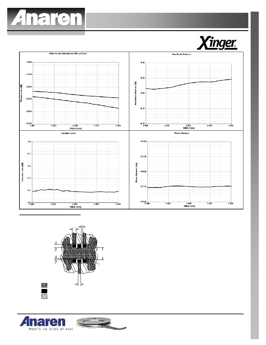
Typical Performance: 2.4 GHz.
to
2.5
GHz.
Mounting Configuration:
FB650 Rev B Mounting Footprint
Dimensions are in Inches [Millimeters]
6X .030
[0.76]
3X 50
Transmission
Line
.095
[2.41]
6X .022
[0.57]
2X .009
[0.22]
Multiple
plated thru holes
to ground
Solder Resist
Footprint Pad (s)
Circuit Pattern
4X .012
[0.30]
In order for Xinger surface mount components to work
optimally, there must be a 50
transmission line to the
balanced port and 50
transmission lines from the
unbalanced ports. If this condition is not satisfied, amplitude
balance, insertion loss and VSWR may not meet published
specifications.
All of the Xinger components are constructed from ceramic
filled PTFE composites which possess excellent electrical
and mechanical stability having X and Y thermal coefficient
of expansion (CTE) of 17 ppm/
o
C
An example of the PCB footprint used in the testing of these
parts is shown to the left. in specific designs, the
transmission line widths need to be adjusted to the unique
dielectric coefficients and thicknesses as well as
varying
pick and place equipment tolerances.
USA/Canada:
Toll Free:
Europe:
(315) 432-8909
(800) 544-2414
+44 2392-232392
Available on Tape and
Reel For Pick and Place
Manufacturing.
Model FB650
Rev. B
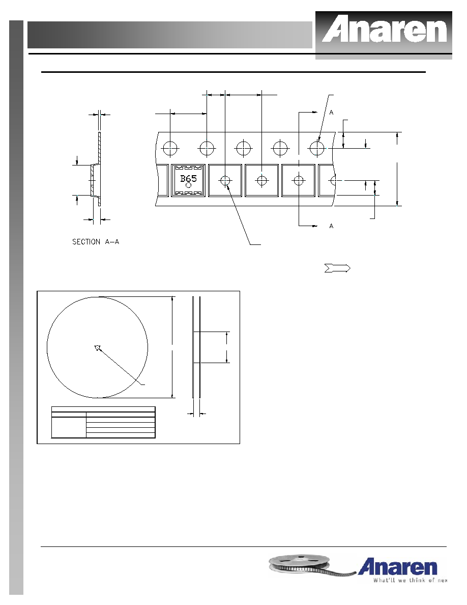
Carrier Tape _
Parts are oriented in embossed tape as shown below
.157
[4.00]
.079 [2.01]
.157
[4.00]
Ø.059
[Ø1.50]
.069
[1.75]
.138
[3.50]
.063
[1.61]
Ø.039
[Ø0.99]
Dimensions are in inches [mm]
Direction of
Part Feed
(Unloading)
.315
[8.00]
.010
[0.25]
.030
[0.80]
.130
[3.30]
Reel
B
ØA
ØC
REEL DIMENSIONS (inches [mm])
ØA
B
ØC
0.32 [8.0]
2.0 [50.8]
7.00 [177.8]
4000
QUANTITY/REEL
TABLE 1
ØD
0.512 [13.0]
ØD