
03/2004
AWT6137
HELP
TM
Cellular Dual Mode AMPS/CDMA
3.4V/28dBm Linear Power Amplifier Module
PRELIMINARY DATA SHEET - Rev 1.0
M7 Package
10 Pin 4 x 4 x 1.5 mm
Surface Mount Module
FEATURES
∑
InGaP HBT Technology
∑
High Efficiency:
39% @ +28 dBm
20% @ +16 dBm
∑
Low Quiescent Current: 15 mA
∑
Low Leakage Current in Shutdown Mode: <1
µ
A
∑
V
REF
= +2.85 V (+2.7 V Min Over Temp.)
∑
Low Profile Surface Mount Package: 1.56mm Max
∑
CDMA 1XRTT and 1xEV-DO Compliant
APPLICATIONS
∑
Single Mode CDMA Wireless Handsets
∑
Dual Mode AMPS/CDMA Wireless Handsets
PRODUCT DESCRIPTION
The AWT6137 CDMA/AMPS Power Amplifier is a high
performance CDMA2000/ 1XRTT amplifier designed
specifically for Cellular wireless applications. This
rugged, easy to use InGaP HBT design delivers
state of the art efficiency and temperature stability
with very low DC power consumption. The
AWT6137 PA module has the lowest CDG currents
available to handset manufacturers today.
A combination of low idle current and mode
switching enables the AWT6137 to deliver
unparalleled CDMA average power efficiencies.
This bias feature allows the AWT6137 to significantly
increase the battery usage time of a mobile
handset. The device has mode-switching to take
advantage of its high efficiency operation over a wide
range of output powers. Higher low power efficiency
is achieved without an external DAC or DC-DC
converter. The integrated power amplifier module
employs a proprietary bias control and temperature
compensation circuit that assures stable operation,
even at extreme temperature conditions.
The self contained 4 x 4 x 1.5 mm surface mount
package incorporates matching networks optimized
for output power, efficiency and linearity in a 50
system making it easy to incorporate the device into
BOTH new and existing designs.
Figure 1: Block Diagram
AWT6137
Bias Control
V
CC
V
REF
RF
IN
RF
OUT
GND
V
MODE
1
7
5
8
10
6
GND at slug (pad)
3
9
4
2
GND
V
CC
GND
GND
PRELIMINARY DATA SHEET - Rev 1.0
03/2004
AWT6137
3
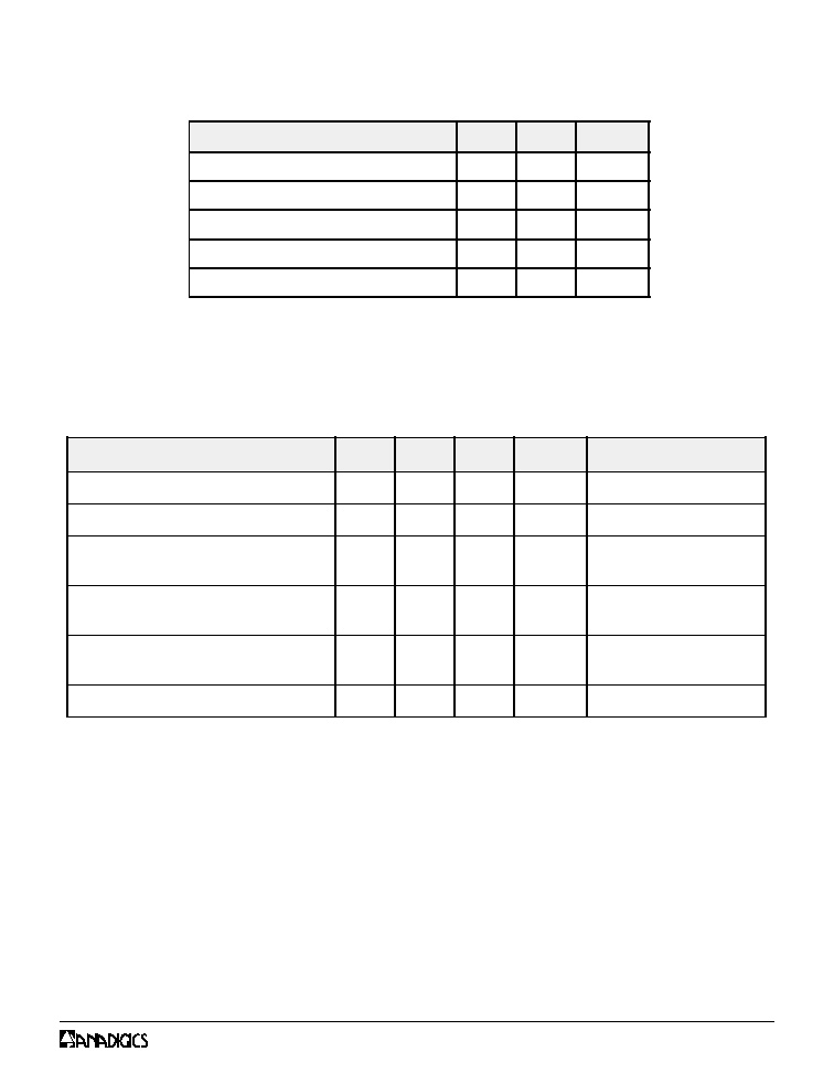
ELECTRICAL CHARACTERISTICS
Table 2: Absolute Minimum and Maximum Ratings
Stresses in excess of the absolute ratings may cause permanent
damage. Functional operation is not implied under these conditions.
Exposure to absolute ratings for extended periods of time may
adversely affect reliability.
Table 3: Operating Ranges
The device may be operated safely over these conditions; however, parametric performance is guaranteed
only over the conditions defined in the electrical specifications.
R
E
T
E
M
A
R
A
P
N
I
M
X
A
M
T
I
N
U
V
(
e
g
a
tl
o
V
y
l
p
p
u
S
C
C
)
0
5
+
V
V
(
e
g
a
tl
o
V
l
o
r
t
n
o
C
e
d
o
M
E
D
O
M
)
0
5
.
3
+
V
V
(
e
g
a
tl
o
V
e
c
n
e
r
e
f
e
R
F
E
R
)
0
5
.
3
+
V
P
(
r
e
w
o
P
t
u
p
n
I
F
R
N
I
)
-
0
1
+
m
B
d
T
(
e
r
u
t
a
r
e
p
m
e
T
e
g
a
r
o
t
S
G
T
S
)
0
4
-
0
5
1
+
C
∞
Notes:
(1) For operation at T
C
= +85
o
C and V
CC
= +3.2 V, P
OUT
is derated by 0.5 dB.
R
E
T
E
M
A
R
A
P
N
I
M
P
Y
T
X
A
M
T
I
N
U
S
T
N
E
M
M
O
C
)
f
(
y
c
n
e
u
q
e
r
F
g
n
it
a
r
e
p
O
4
2
8
-
9
4
8
z
H
M
V
(
e
g
a
tl
o
V
y
l
p
p
u
S
C
C
)
2
.
3
+
4
.
3
+
2
.
4
+
V
V
(
e
g
a
tl
o
V
e
c
n
e
r
e
f
e
R
F
E
R
)
7
.
2
+
0
5
8
.
2
+
-
1
.
3
+
5
.
0
+
V
"
n
o
"
A
P
"
n
w
o
d
t
u
h
s
"
A
P
V
(
e
g
a
tl
o
V
l
o
r
t
n
o
C
e
d
o
M
E
D
O
M
)
5
.
2
+
0
5
8
.
2
+
-
1
.
3
+
5
.
0
+
V
e
d
o
M
s
a
i
B
w
o
L
e
d
o
M
s
a
i
B
h
g
i
H
P
(
r
e
w
o
P
t
u
p
t
u
O
F
R
T
U
O
)
5
.
0
3
)
1
(
5
.
7
2
)
1
(
0
.
1
3
0
.
8
2
-
-
m
B
d
S
P
M
A
A
M
D
C
T
(
e
r
u
t
a
r
e
p
m
e
T
e
s
a
C
C
)
0
3
-
-
5
8
+
C
∞

PRELIMINARY DATA SHEET - Rev 1.0
03/2004
AWT6137
5
Table 5: Electrical Specifications - CDMA Operation
(T
C
= +25 ∞C, V
CC
= +3.4 V, V
REF
= +2.85 V, 50
system)
Notes:
(1) PAE and ACP limit applies at 836.5 MHz.
R
E
T
E
M
A
R
A
P
N
I
M
P
Y
T
X
A
M
T
I
N
U
S
T
N
E
M
M
O
C
n
i
a
G
5
2
4
1
7
2
6
1
0
3
0
2
B
d
P
T
U
O
V
,
m
B
d
8
2
+
=
E
D
O
M
V
0
=
P
T
U
O
V
,
m
B
d
6
1
+
=
E
D
O
M
V
5
8
.
2
+
=
r
e
w
o
P
l
e
n
n
a
h
C
t
n
e
c
a
j
d
A
t
a +
t
e
s
ff
o
z
H
k
5
8
8
)
1
(
z
H
M
3
2
.
1
=
W
B
l
e
n
n
a
h
C
y
r
a
m
ir
P
z
H
k
0
3
=
W
B
l
e
n
n
a
h
C
t
n
e
c
a
j
d
A
-
-
9
4
-
4
5
-
7
4
-
7
4
-
c
B
d
P
T
U
O
V
,
m
B
d
8
2
+
=
E
D
O
M
V
0
=
P
T
U
O
V
,
m
B
d
6
1
+
=
E
D
O
M
V
5
8
.
2
+
=
r
e
w
o
P
l
e
n
n
a
h
C
t
n
e
c
a
j
d
A
t
a +
t
e
s
ff
o
z
H
M
8
9
.
1
z
H
M
3
2
.
1
=
W
B
l
e
n
n
a
h
C
y
r
a
m
ir
P
z
H
k
0
3
=
W
B
l
e
n
n
a
h
C
t
n
e
c
a
j
d
A
-
-
9
5
-
0
6
-
6
5
-
7
5
-
c
B
d
P
T
U
O
V
,
m
B
d
8
2
+
=
E
D
O
M
V
0
=
P
T
U
O
V
,
m
B
d
6
1
+
=
E
D
O
M
V
5
8
.
2
+
=
y
c
n
e
i
c
if
f
E
d
e
d
d
A
-
r
e
w
o
P
)
1
(
7
3
8
1
1
9
3
0
2
7
.
1
-
-
-
%
P
T
U
O
V
,
m
B
d
8
2
+
=
E
D
O
M
V
0
=
P
T
U
O
V
,
m
B
d
6
1
+
=
E
D
O
M
V
5
8
.
2
+
=
P
T
U
O
V
,
m
B
d
0
=
E
D
O
M
V
5
8
.
2
+
=
)
q
c
I
(
t
n
e
r
r
u
C
t
n
e
c
s
e
i
u
Q
-
-
0
0
1
5
1
0
2
1
0
2
A
m
V
E
D
O
M
V
0
=
V
E
D
O
M
V
5
8
.
2
+
=
t
n
e
r
r
u
C
e
c
n
e
r
e
f
e
R
-
5
.
3
0
.
5
A
m
V
h
g
u
o
r
h
t
F
E
R
n
i
p
t
n
e
r
r
u
C
l
o
r
t
n
o
C
e
d
o
M
-
6
.
0
1
A
m
V
h
g
u
o
r
h
t
E
D
O
M
n
i
p
t
n
e
r
r
u
C
e
g
a
k
a
e
L
-
1
<
5
A
µ
V
C
C
V
,
V
2
.
4
+
=
F
E
R
,
V
0
=
V
E
D
O
M
V
0
=
d
n
a
B
e
v
i
e
c
e
R
n
i
e
s
i
o
N
-
5
3
1
-
3
3
1
-
z
H
/
m
B
d
z
H
M
4
9
8
o
t
z
H
M
9
6
8
s
c
i
n
o
m
r
a
H
o
f
2
o
f
4
,
o
f
3
-
-
0
4
-
5
4
-
0
3
-
0
3
-
c
B
d
e
c
n
a
d
e
p
m
I
t
u
p
n
I
-
-
1
:
2
R
W
S
V
l
e
v
e
L
t
u
p
t
u
O
s
u
o
ir
u
p
S
)
s
t
u
p
t
u
o
s
u
o
ir
u
p
s
ll
a
(
-
-
5
6
-
c
B
d
P
T
U
O
<
m
B
d
8
2
+
1
:
5
<
R
W
S
V
d
a
o
l
d
n
a
b
-
n
I
1
:
0
1
<
R
W
S
V
d
a
o
l
d
n
a
b
-
f
o
-
t
u
O
o
n
h
ti
w
s
s
e
r
t
s
h
c
t
a
m
s
i
m
d
a
o
L
e
r
u
li
a
f
r
o
n
o
it
a
d
a
r
g
e
d
t
n
e
n
a
m
r
e
p
1
:
8
-
-
R
W
S
V
V
C
C
V
0
.
5
+
=
P
N
I
m
B
d
5
+
=
g
n
it
a
r
e
p
o
ll
u
f
r
e
v
o
s
e
il
p
p
A
e
g
n
a
r
e
r
u
t
a
r
e
p
m
e
t

