
03/2006
AWT6136
450 MHz CDMA 3.4V/29.5dBm
Linear Power Amplifier Module
PRELIMINARY DATA SHEET - Rev 1.6
M5 Package
7 Pin 6 mm x 6 mm x 1.5 mm
Surface Mount Module
FEATURES
∑
InGaP HBT Technology
∑
High Efficiency 37% CDMA
∑
Low Receive Band Noise (NR
X
) -132 dBm/Hz @
10 MHz offset
∑
Low Leakage Current (<5
µ
A)
∑
SMT Module Package
∑
Small Foot Print (6 mm x 6 mm)
∑
50
Input and Output Matching
∑
Low Quiescent Current (Icq = 60 mA Typ)
∑
Shut Down and Mode Control
∑
CDMA 2000 1XRTT Compliant
∑
RoHS Compliant Package Option, 250
o
C MSL-3
APPLICATIONS
∑
450 MHz Single Mode CDMA Wireless
Handsets and Wireless Local Loop
PRODUCT DESCRIPTION
The AWT6136 is a high power, high efficiency
amplifier module for CDMA wireless handset
applications. The device is manufactured on an
advanced InGaP HBT MMIC technology offering
state-of-the-art reliability, temperature stability and
ruggedness. A low power quiescent current mode
is digitally controlled to reduce power drain on the
system battery. The 6 mm x 6 mm x 1.5 mm laminate
package is self contained, incorporating 50
input
and output matching networks optimized for output
power, linearity, and efficiency.
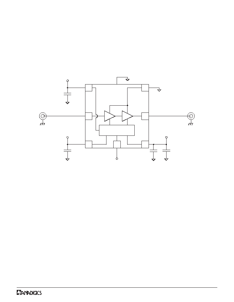
Figure 1: Block Diagram
Bias Control
V
CC
V
REF
RF
IN
V
CC
GND
V
MODE
1
4
3
6
7
2
5
GND at slug (pad)
RF
OUT
AWT6136

PRELIMINARY DATA SHEET - Rev 1.6
03/2006
AWT6136
3
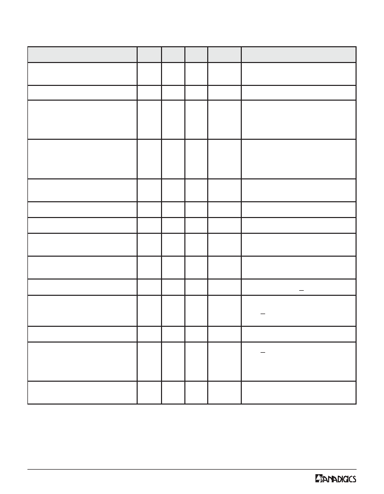
ELECTRICAL CHARACTERISTICS
Table 2: Absolute Minimum and Maximum Ratings
Stresses in excess of the absolute ratings may cause permanent
damage. Functional operation is not implied under these conditions.
Exposure to absolute ratings for extended periods of time may
adversely affect reliability.
R
E
T
E
M
A
R
A
P
N
I
M
X
A
M
T
I
N
U
V
(
e
g
a
tl
o
V
y
l
p
p
u
S
C
C
)
0
5
+
V
V
(
e
g
a
tl
o
V
l
o
r
t
n
o
C
e
d
o
M
E
D
O
M
)
0
4
.
3
+
V
V
(
e
g
a
tl
o
V
e
c
n
e
r
e
f
e
R
F
E
R
)
0
4
.
3
+
V
P
(
r
e
w
o
P
t
u
p
n
I
F
R
N
I
)
-
0
1
+
m
B
d
T
(
e
r
u
t
a
r
e
p
m
e
T
e
g
a
r
o
t
S
G
T
S
)
0
4
-
0
5
1
+
C
∞
Table 3: Operating Ranges
The device may be operated safely over these conditions; however, parametric performance is
guaranteed only over the conditions defined in the electrical specifications.
Notes:
(1) For operation at V
CC
= +3.2 V and T
C
= +90
O
C, P
OUT
is derated by 0.5 dB.
R
E
T
E
M
A
R
A
P
N
I
M
P
Y
T
X
A
M
T
I
N
U
S
T
N
E
M
M
O
C
)
f
(
y
c
n
e
u
q
e
r
F
g
n
it
a
r
e
p
O
0
5
4
-
0
6
4
z
H
M
V
(
e
g
a
tl
o
V
y
l
p
p
u
S
C
C
)
2
.
3
+
4
.
3
+
2
.
4
+
V
V
(
e
g
a
tl
o
V
e
c
n
e
r
e
f
e
R
F
E
R
)
0
8
.
2
+
0
0
9
.
2
+
-
1
.
3
+
5
.
0
+
V
"
n
o
"
A
P
"
n
w
o
d
t
u
h
s
"
A
P
V
(
e
g
a
tl
o
V
l
o
r
t
n
o
C
e
d
o
M
E
D
O
M
)
5
.
2
+
0
0
9
.
2
+
-
1
.
3
+
5
.
0
+
V
e
d
o
M
s
a
i
B
w
o
L
e
d
o
M
s
a
i
B
h
g
i
H
P
(
r
e
w
o
P
t
u
p
t
u
O
F
R
T
U
O
)
0
.
9
2
+
)
1
(
5
.
9
2
+
-
m
B
d
V
,
A
M
D
C
C
C
V
4
.
3
+
=
T
(
e
r
u
t
a
r
e
p
m
e
T
e
s
a
C
C
)
0
1
-
-
0
9
+
o
C
4
PRELIMINARY DATA SHEET - Rev 1.6
03/2006
AWT6136
Table 4: Electrical Specifications ≠ CDMA Operation
(T
C
= +25
O
C, V
CC
= +3.4 V, V
REF
= +2.90 V, 50
system)
Notes:
(1) P
OUT
is derated by 0.5 dB for IS-98 / CDMA 2000 operation.
(2) Efficiency spec applies at 455 MHz.
R
E
T
E
M
A
R
A
P
N
I
M
P
Y
T
X
A
M
T
I
N
U
S
T
N
E
M
M
O
C
n
i
a
G
6
2
5
2
5
.
8
2
5
.
7
2
0
3
9
2
B
d
P
OUT
V
,
m
B
d
5
.
9
2
+
=
MODE
V
0
=
P
OUT
V
,
m
B
d
6
1
+
=
MODE
V
0
9
.
2
+
=
n
o
it
a
ir
a
V
n
i
a
G
-
4
.
0
0
.
1
B
d
r
e
w
o
P
l
e
n
n
a
h
C
t
n
e
c
a
j
d
A
t
a
±
t
e
s
ff
o
z
H
k
5
8
8
)
1
(
Z
H
M
3
2
.
1
=
W
B
l
e
n
n
a
h
C
y
r
a
m
ir
P
z
H
k
0
3
=
W
B
l
e
n
n
a
h
C
t
n
e
c
a
j
d
A
-
-
0
5
-
8
5
-
7
4
-
7
4
-
B
d
P
OUT
V
,
m
B
d
5
.
9
2
+
=
MODE
V
0
=
P
OUT
V
,
m
B
d
6
1
+
=
MODE
V
0
9
.
2
+
=
r
e
w
o
P
l
e
n
n
a
h
C
t
n
e
c
a
j
d
A
t
a
±
t
e
s
ff
o
z
H
M
8
9
.
1
)
1
(
Z
H
M
3
2
.
1
=
W
B
l
e
n
n
a
h
C
y
r
a
m
ir
P
z
H
k
0
3
=
W
B
l
e
n
n
a
h
C
t
n
e
c
a
j
d
A
-
-
2
6
-
8
6
-
9
5
-
9
5
-
B
d
P
OUT
V
,
m
B
d
5
.
9
2
+
=
MODE
V
0
=
P
OUT
V
,
m
B
d
6
1
+
=
MODE
V
0
9
.
2
+
=
y
c
n
e
i
c
if
f
E
d
e
d
d
A
-
r
e
w
o
P
)
2
(
,
)
1
(
3
3
6
7
3
7
-
-
%
P
OUT
V
,
m
B
d
5
.
9
2
+
=
MODE
V
0
=
P
OUT
V
,
m
B
d
6
1
+
=
MODE
V
0
9
.
2
+
=
)
q
c
I
(
t
n
e
r
r
u
C
t
n
e
c
s
e
i
u
Q
-
1
6
5
7
A
m
V
h
g
u
o
r
h
t
C
C
V
,
s
n
i
p
MODE
V
0
9
.
2
+
=
t
n
e
r
r
u
C
e
c
n
e
r
e
f
e
R
-
5
.
6
9
A
m
V
h
g
u
o
r
h
t
REF
"
n
o
"
A
P
,
n
i
p
t
n
e
r
r
u
C
l
o
r
t
n
o
C
e
d
o
M
-
8
.
0
0
.
1
A
m
V
h
g
u
o
r
h
t
MODE
,
n
i
p
V
MODE
V
0
9
.
2
+
=
t
n
e
r
r
u
C
e
g
a
k
a
e
L
-
1
<
5
µ
A
V
C
C
V
,
V
2
.
4
+
=
REF
,
V
0
=
V
MODE
V
0
=
d
n
a
B
e
v
i
e
c
e
R
n
i
e
s
i
o
N
-
2
3
1
-
0
3
1
-
z
H
/
m
B
d
f
O
P
,
z
H
M
0
1
+
OUT
<
m
B
d
5
.
9
2
+
s
c
i
n
o
m
r
a
H
o
f
2
o
f
4
,
o
f
3
-
-
6
3
-
4
4
-
0
3
-
5
3
-
c
B
d
P
OUT
<
m
B
d
5
.
9
2
+
e
c
n
a
d
e
p
m
I
t
u
p
n
I
-
-
1
:
2
R
W
S
V
l
e
v
e
L
t
u
p
t
u
O
s
u
o
ir
u
p
S
)
s
t
u
p
t
u
o
s
u
o
ir
u
p
s
ll
a
(
-
-
0
7
-
c
B
d
P
OUT
<
m
B
d
5
.
9
2
+
1
:
5
<
R
W
S
V
d
a
o
L
d
n
a
b
-
n
I
1
:
0
1
<
R
W
S
V
d
a
o
L
d
n
a
b
-
f
o
-
t
u
O
s
e
g
n
a
r
g
n
it
a
r
e
p
o
ll
a
r
e
v
o
s
e
il
p
p
A
o
n
h
ti
w
s
s
e
r
t
s
h
c
t
a
m
s
i
m
d
a
o
L
e
r
u
li
a
f
r
o
n
o
it
a
d
a
r
g
e
d
t
n
e
n
a
m
r
e
p
1
:
0
1
-
-
R
W
S
V
s
e
g
n
a
r
g
n
it
a
r
e
p
o
ll
a
r
e
v
o
s
e
il
p
p
A
PRELIMINARY DATA SHEET - Rev 1.6
03/2006
AWT6136
5
APPLICATION INFORMATION
To ensure proper performance, refer to all related
Application Notes on the ANADIGICS web site:
http://www.anadigics.com
Shutdown Mode
The power amplifier may be placed in a shutdown
mode by applying logic low levels (see Operating
Ranges table) to both the V
REF
and V
MODE
voltages.
Figure 3: Application Circuit Schematic
(50 Ohms)
(50 Ohms)
RF Input
4.7uF
0.1uF
4.7uF (ceramic)
GND at slug (pad)
Bias Control
1
4
3
6
7
2
5
GND
V
CC
V
CC
V
REF
V
MODE
RF Out
(ceramic)
4.7uF
High Bias Mode
The power amplifier may be placed in a high bias
mode by applying a logic low level (see Operating
Ranges table) to the V
MODE
voltage.
