 | –≠–ª–µ–∫—Ç—Ä–æ–Ω–Ω—ã–π –∫–æ–º–ø–æ–Ω–µ–Ω—Ç: AWT6123 | –°–∫–∞—á–∞—Ç—å:  PDF PDF  ZIP ZIP |

02-2003
Figure 1: Block Diagram
FEATURES
∑
InGaP HBT Technology
∑
+35dBm GSM Output Power at 3.5V
∑
+32.5dBm DCS/PCS Output Power at 3.5V
∑
35% GSM850 PAE (Class 5)
∑
50% GSM850 PAE (Class 4)
∑
55% GSM900 PAE
∑
50% DCS/PCS PAE
∑
Low Profile 1.4mm Package
∑
Small footprint 6 x 8mm SMT Package
∑
GPRS Capable (class 12)
APPLICATIONS
GSM850/GSM900/DCS/PCS Handsets
Dual/Tri/Quad Band PDA
PRODUCT DESCRIPTION
ANADIGICS is introducing two 3-stage power
amplifiers designed for high performance in Quad
Band Applications. The amplifiers are packaged in
a very small 6 x 8mm module. The output power is
controlled by changing the voltage applied to the
V
APC
pin for each amplifier. The part is shut down by
removing the regulated supply voltage.
The amplifier is manufactured using an advanced
InGaP HBT technology, offering state of the art
reliability, temperature stability and ruggedness.
Passive matching networks are integrated to
provide internal matching to 50
at both the RF
inputs and outputs. Internal DC blocks are pro-
vided at the RF inputs.
AWT6123
GSM850/GSM900/DCS/PCS
Quad Band Power Amplifier
Advanced Product Information Rev 0.7
GSM_IN
DCS/PCS Bias
V
APC_DCS/PCS
V
CCB
GSM_OUT
DCS/PCS_IN
DCS/PCS_OUT
V
REG_DCS/PCS
V
APC_GSM
V
REG_GSM
GSM Bias
V
CCA_DCS/PCS
V
CCA_GSM
2
Advanced Product Information - Rev 0.7
02-2003
AWT6123
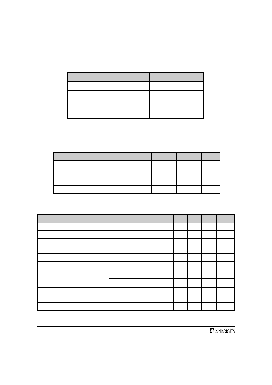
PARAMETER
MIN
MAX
UNITS
Supply Voltage (V
CC
)
+7
V
RF Input Power (RF
IN
)
+14
dBm
Control Voltage (V
APC
)
3.0
V
Storage Temperature (T
STG
)
-55
150
∞C
Stresses in excess of the absolute ratings may cause permanent damage.
Functional operation is not implied under these conditions. Exposure to
absolute ratings for extended periods of time may adversely affect
reliability.
ELECTRICAL CHARACTERISTICS
Table 1: Absolute Maximum Ratings
Table 2: ESD Ratings
PARAMETER
METHOD
RATING
UNITS
ESD threshold voltage (RF ports)
HBM
250
V
ESD threshold voltage (control inputs)
HBM
250
V
ESD threshold voltage (RF inputs)
CDM
TBD
V
ESD threshold voltage (control inputs)
CDM
TBD
V
Table 3: Operating Conditions
Note 1: The V
APC
must be pulled down to 0.45V with a low impedance. If V
REG_GSM
& V
REG_DCS/PCS
inputs
are connected then both V
APC
inputs must be pulled down to 0.45V to disable both power amplifiers.
PARAMETER
CONDITIONS
MIN
TYP
MAX UNITS
Supply voltage (V
CC
)
3.0
3.5
4.2
V
Regulated voltage (V
REG
)
2.7
2.8
3.0
V
Individual Regulated current (I
REG
)
V
REG_GSM
or V
REG_DCS/PCS
= 3.0V
3.5
4.5
mA
Control voltage (V
APC
)
0.45
V
REG
V
Control Voltage (V
APC
) for max power
1.8
2.2
V
Individual Control current (I
APC
)
See Note 1
V
APC
= 0.45V
-3
mA
V
APC
= 2.2V
3
mA
V
APC
= 3.0V
6
mA
Leakage current
V
CC
= 4.2V, No RF Applied
V
REG_GSM
= V
REG_DCS/PCS
= 0V
0
10
A
Case temperature (T
C
)
-20
85
∞C
µ

Advanced Product Information - Rev 0.7
02-2003
3
AWT6123
Note: Power control outputs need to sink current to power down each power amplifier
Figure 3: Application Block Diagram For Single Output Power Control
GSM_IN
DCS/PCS Bias
V
APC_DCS/PCS
V
CCB
GSM_OUT
DCS/PCS_IN
DCS/PCS_OUT
V
REG_DCS/PCS
Power Control IC
V
APC_GSM
V
REG_GSM
GSM Bias
V
CCA_DCS/PCS
V
CCA_GSM
Reg
Reg
To
Filter/
Switch
Vramp
EN_A
EN_B
~3.5mA
~3.5mA
-3.0 to +3.0mA
Figure 4: Application Block Diagram For Dual Output Power Control
BAND
EN_A
EN_B
GSM800/900
OFF
ON
DCS/PCS
ON
OFF
GSM_IN
DCS/PCS Bias
V
APC_DCS/PCS
V
CCB
GSM_OUT
DCS/PCS_IN
DCS/PCS_OUT
V
REG_DCS/PCS
V
APC_GSM
V
REG_GSM
GSM Bias
V
CCA_DCS/PCS
V
CCA_GSM
Reg
EN
Vramp
Power Control IC
~7mA
-3.0 to +3.0mA
-3.0 to +3.0mA
To
Filter/
Switch
To
Filter/
Switch

4
Advanced Product Information - Rev 0.7
02-2003
AWT6123
Table 4: Electrical Characteristics for GSM850/900
Unless otherwise specified:V
CC
= 3.5V, P
IN
= 5.5dBm, V
REG_GSM
= 2.8V, V
APC_GSM
= 2.2V, Z
IN
= Z
OUT
= 50
, T
C
= 25 ∞C
V
REG_DCS/PCS
= V
APC_DCS/PCS
= 0V, Pulse Width =1154
µ
s
PARAMETER
SYMBOL
CONDITIONS
MIN
TYP
MAX
UNIT
Operating Frequency
F
IN
824
880
849
915
MHz
MHz
Input Power
P
IN
3
5.5
8
dBm
GSM850 Band (824 to 849MHz)
Output Power
P
MAX
34.5
35
dBm
Efficiency GSM850 Class 4
PAE
P
OUT
= P
MAX
45
50
%
Efficiency GSM850 Class 5
PAE
P
OUT
= 31.5dBm
35
%
Degraded Output Power
V
CC
= 3.0V, V
REG
= 2.7V,
T
C
= 85∞C, P
IN
= 3dBm
32.5
dBm
GSM900 Band (880 to 915MHz)
Output Power
P
MAX
34.5
35
dBm
Efficiency GSM900 Class 4
PAE
P
OUT
= P
MAX
50
55
%
Degraded Output Power
V
CC
= 3.0V, V
REG
= 2.7V,
T
C
= 85∞C, P
IN
= 3dBm
32.5
dBm
All Bands
Isolation
V
APC
= 0.45V, P
IN
= 8dBm
-35
-30
dBm
Cross Isolation
2*F
IN
at DCS/PCS_OUT
port, DCS/PCS PA = OFF
-20
dBm
Harmonics (2-14F)
V
APC
= 0.45 to 2.2V
-12
-7
dBm
Stability
All V
APC
, All V
CC
, All V
REG
,
T
C
= -20 to 85∞C,
VSWR = 8:1 All phases
-36
dBm
Ruggedness
All V
APC
, All V
CC
, All V
REG
,
T
C
= -20 to 85∞C, All phases
10:1
ratio
RX Band Noise Power
RBW=VBW=100kHz,
P
IN
= 3.0 to 8dBm,
F
IN
= 915MHz,
F
OUT
= F
IN
+ 10 to 20MHz
-70
dBm
RBW=VBW=100kHz,
P
IN
= 3.0 to 8dBm,
F
IN
= 849 or 915MHz,
F
OUT
= F
IN
+ 20 to 45MHz
-82
dBm
Input Return Loss
P
OUT
= 5dBm to P
MAX
2.5:1

Advanced Product Information - Rev 0.7
02-2003
5
AWT6123
Table 5: Electrical Characteristics for DCS/PCS
PARAMETER
SYMBOL
CONDITIONS
MIN
TYP
MAX
UNIT
Operating Frequency
F
IN
1710
1850
1785
1910
MHz
MHz
Input Power
P
IN
3
5.5
8
dBm
Output Power
P
MAX
F
IN
= 1710 to 1785MHz
32.0
32.5
dBm
F
IN
= 1850 to 1910MHz
32.0
32.5
dBm
Degraded Output Power
V
CC
= 3.0V, V
REG
= 2.7V,
T
C
= 85∞C
F
IN
= 1710 to 1785MHz
29.5
dBm
V
CC
= 3.0V, V
REG
= 2.7V,
T
C
= 85∞C
F
IN
= 1880 to 1910MHz
29.5
dBm
Efficiency
(P
OUT
=P
MAX
)
F
IN
= 1710 to 1910MHz
45
50
%
Isolation
V
APC
= 0.45V, P
IN
= 8dBm
-35
-30
dBm
Harmonics (2-7F)
V
APC
= 0.45 to 2.2V
-12
-7
dBm
Stability
All V
APC
, All V
CC
, All V
REG
,
T
C
= -20 to 85∞C,
VSWR = 8:1 All phases
-36
dBm
Ruggedness
All V
APC
, All V
CC
, All V
REG
,
T
C
= -20 to 85∞C,
All phases
10:1
ratio
RX Band Noise Power
RBW=VBW=100kHz,
P
IN
= 3.0 to 8.0dBm,
F
IN
= 1785 or 1910MHz,
F
OUT
= F
IN
+ 20 to 95MHz
-80
-74
dBm
Input Return Loss
P
OUT
= 0dBm to P
MAX
2.5:1
Unless otherwise specified:
V
CC
= 3.5V, P
IN
= 5.5dBm, V
REG_DCS/PCS
= 2.8V, V
APC_DCS/PCS
= 2.2V, Z
IN
= Z
OUT
= 50
, T
C
= 25 ∞C
V
REG_GSM
= V
APC_GSM
= 0V, Pulse Width =1154
µ
s