06/2005
AWT6112
Cellular Dual Mode AMPS/CDMA
3.4V/28dBm Linear Power Amplifier Module
PRELIMINARY DATA SHEET - Rev 1.6
M7 Package
10 Pin 4 mm x 4 mm x 1.5 mm
Surface Mount Module
FEATURES
∑
InGaP HBT Technology
∑
High Efficiency: 54% AMPS, 38% CDMA
∑
Low Quiescent Current: 50 mA
∑
Low Leakage Current in Shutdown Mode: <5
µ
A
∑
Optimized for a 50
System
∑
Low Profile Surface Mount Package: 1.56mm Max
∑
CDMA 1XRTT Compliant
∑
CDMA 1xEV-DO Compliant
∑
RoHS Compliant Package Option, 250
o
C MSL-3
APPLICATIONS
∑
Single Mode CDMA Wireless Handsets
∑
Dual Mode AMPS/CDMA Wireless Handsets
PRODUCT DESCRIPTION
The AWT6112 is a high power, high efficiency
amplifier module for dual mode AMPS/CDMA
wireless handset applications. The device is
manufactured on an advanced InGaP HBT MMIC
technology offering state-of-the-art reliability,
temperature stability, and ruggedness. Selectable
bias modes that optimize efficiency for different
output power levels, and a shutdown mode with low
leakage current, serve to increase handset talk and
standby time. The self contained 4 mm x 4 mm x 1.5 mm
surface mount package incorporates matching
networks optimized for output power, efficiency and
linearity in a 50
system.
Figure 1: Block Diagram
Bias Control
V
CC
V
REF
RF
IN
RF
OUT
GND
V
MODE
1
7
5
8
10
6
GND at slug (pad)
3
9
4
2
GND
V
CC
GND
GND
PRELIMINARY DATA SHEET - Rev 1.6
06/2005
AWT6112
3
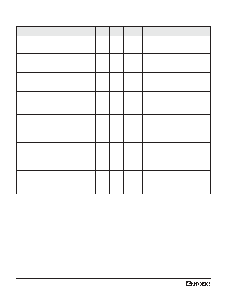
ELECTRICAL CHARACTERISTICS
Table 2: Absolute Minimum and Maximum Ratings
Stresses in excess of the absolute ratings may cause permanent
damage. Functional operation is not implied under these conditions.
Exposure to absolute ratings for extended periods of time may
adversely affect reliability.
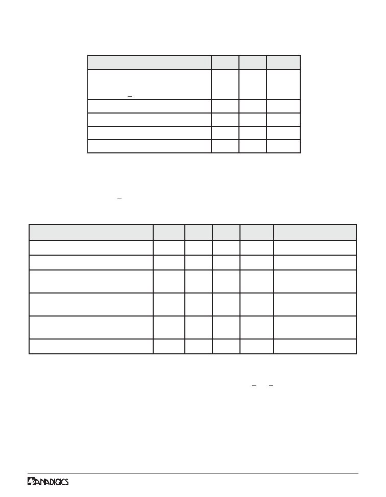
Table 3: Operating Ranges
The device may be operated safely over these conditions; however, parametric performance is guaranteed
only over the conditions defined in the electrical specifications.
R
E
T
E
M
A
R
A
P
N
I
M
P
Y
T
X
A
M
T
I
N
U
S
T
N
E
M
M
O
C
)
f
(
y
c
n
e
u
q
e
r
F
g
n
it
a
r
e
p
O
4
2
8
-
9
4
8
z
H
M
V
(
e
g
a
tl
o
V
y
l
p
p
u
S
C
C
)
2
.
3
+
4
.
3
+
2
.
4
+
V
V
(
e
g
a
tl
o
V
e
c
n
e
r
e
f
e
R
F
E
R
)
5
7
.
2
+
0
5
8
.
2
+
-
1
.
3
+
5
.
0
+
V
"
n
o
"
A
P
"
n
w
o
d
t
u
h
s
"
A
P
V
(
e
g
a
tl
o
V
l
o
r
t
n
o
C
e
d
o
M
E
D
O
M
)
5
.
2
+
0
5
8
.
2
+
-
1
.
3
+
5
.
0
+
V
e
d
o
M
s
a
i
B
w
o
L
e
d
o
M
s
a
i
B
h
g
i
H
P
(
r
e
w
o
P
t
u
p
t
u
O
F
R
T
U
O
)
5
.
0
3
+
)
1
(
5
.
7
2
+
)
1
(
0
.
1
3
+
0
.
8
2
+
-
-
m
B
d
e
d
o
M
S
P
M
A
e
d
o
M
A
M
D
C
T
(
e
r
u
t
a
r
e
p
m
e
T
e
s
a
C
C
)
0
3
-
-
5
8
+
C
∞
Notes:
(1) For operation at T
C
= 100 ∞C, P
OUT
is derated an additional 0.5 dB for +3.2 V < V
CC
< +3.4 V.
R
E
T
E
M
A
R
A
P
N
I
M
X
A
M
T
I
N
U
V
(
e
g
a
tl
o
V
y
l
p
p
u
S
C
C
)
y
l
n
O
C
D
e
v
ir
D
F
R
<
m
B
d
5
+
0
0
8
+
6
+
)
1
(
V
V
(
e
g
a
tl
o
V
l
o
rt
n
o
C
e
d
o
M
E
D
O
M
)
0
5
.
3
+
V
V
(
e
g
a
tl
o
V
e
c
n
e
r
e
f
e
R
F
E
R
)
0
5
.
3
+
V
P
(
r
e
w
o
P
t
u
p
n
I
F
R
N
I
)
-
0
1
+
m
B
d
T
(
e
r
u
t
a
r
e
p
m
e
T
e
g
a
r
o
t
S
G
T
S
)
0
4
-
0
5
1
+
C
∞
Notes:
(1) VSWR < 2:1
PRELIMINARY DATA SHEET - Rev 1.6
06/2005
AWT6112
5
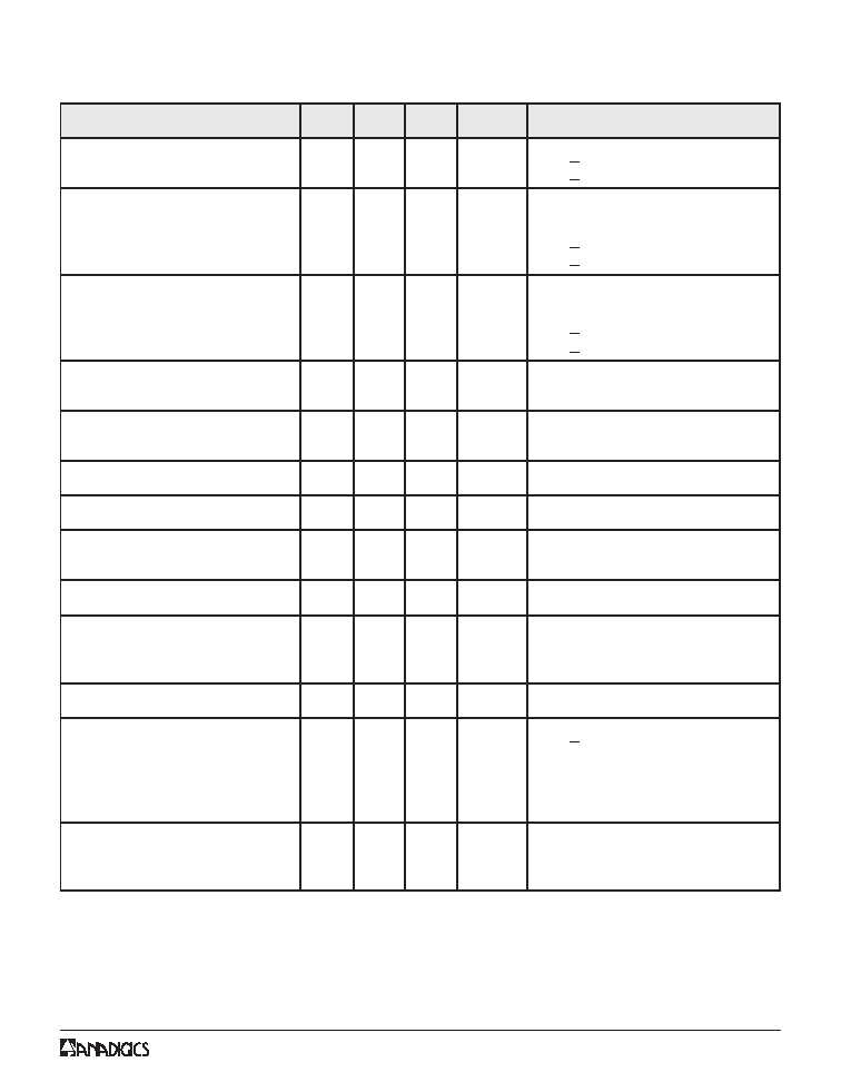
Table 5: Electrical Specifications - CDMA Operation
(T
C
= +25 ∞C, V
CC
= +3.4 V, V
REF
= +2.85 V, 50
system)
Notes:
(1) PAE and ACP limit applies at 836.5 MHz.
R
E
T
E
M
A
R
A
P
N
I
M
P
Y
T
X
A
M
T
I
N
U
S
T
N
E
M
M
O
C
n
i
a
G
6
2
4
2
5
.
7
2
5
.
6
2
0
3
8
2
B
d
P
OUT
<
V
,
m
B
d
8
2
+
MODE
V
0
=
P
OUT
<
V
,
m
B
d
6
1
+
MODE
V
5
8
.
2
=
r
e
w
o
P
l
e
n
n
a
h
C
t
n
e
c
a
j
d
A
t
a 6
t
e
s
ff
o
z
H
k
5
8
8
)
1
(
Z
H
M
3
2
.
1
=
W
B
l
e
n
n
a
h
C
y
r
a
m
ir
P
z
H
k
0
3
=
W
B
l
e
n
n
a
h
C
t
n
e
c
a
j
d
A
-
-
9
4
-
8
4
-
7
4
-
6
4
-
B
d
P
OUT
<
V
,
m
B
d
8
2
+
MODE
V
0
=
P
OUT
<
V
,
m
B
d
6
1
+
MODE
V
5
8
.
2
=
r
e
w
o
P
l
e
n
n
a
h
C
t
n
e
c
a
j
d
A
t
a 6
t
e
s
ff
o
z
H
M
8
9
.
1
Z
H
M
3
2
.
1
=
W
B
l
e
n
n
a
h
C
y
r
a
m
ir
P
z
H
k
0
3
=
W
B
l
e
n
n
a
h
C
t
n
e
c
a
j
d
A
-
-
8
5
-
8
6
-
6
5
-
7
5
-
B
d
P
OUT
<
V
,
m
B
d
8
2
+
MODE
V
0
=
P
OUT
<
V
,
m
B
d
6
1
+
MODE
V
5
8
.
2
=
y
c
n
e
i
c
if
f
E
d
e
d
d
A
-
r
e
w
o
P
)
1
(
7
3
8
5
.
8
3
5
.
8
-
-
%
P
OUT
V
,
m
B
d
8
2
+
=
MODE
V
0
=
P
OUT
V
,
m
B
d
6
1
+
=
MODE
V
5
8
.
2
+
=
)
q
c
I(
t
n
e
r
r
u
C
t
n
e
c
s
e
i
u
Q
-
8
7
9
4
5
9
0
6
A
m
V
MODE
V
0
=
V
MODE
=
5
8
.
2
+
V
t
n
e
r
r
u
C
e
c
n
e
r
e
f
e
R
-
3
.
2
0
.
4
A
m
V
h
g
u
o
r
h
t
REF
n
i
p
t
n
e
r
r
u
C
l
o
rt
n
o
C
e
d
o
M
-
5
3
.
0
7
.
0
A
m
V
h
g
u
o
r
h
t
MODE
,
n
i
p
t
n
e
r
r
u
C
e
g
a
k
a
e
L
-
1
<
5
mA
V
CC
V
,
V
2
.
4
+
=
REF
,
V
0
=
V
MODE
V
0
=
d
n
a
B
e
v
i
e
c
e
R
n
i
e
s
i
o
N
-
5
3
1
-
2
3
1
-
z
H
/
m
B
d
z
H
M
4
9
8
o
t
z
H
M
9
6
8
s
c
i
n
o
m
r
a
H
o
f
2
o
f
4
,
o
f
3
-
-
5
4
-
5
5
-
0
3
-
0
3
-
c
B
d
e
c
n
a
d
e
p
m
I
t
u
p
n
I
-
-
1
:
2
R
W
S
V
l
e
v
e
L
t
u
p
t
u
O
s
u
o
ir
u
p
S
)
s
t
u
p
t
u
o
s
u
o
ir
u
p
s
ll
a
(
-
-
5
6
-
c
B
d
P
OUT
<
m
B
d
8
2
+
1
:
8
<
R
W
S
V
d
a
o
l
d
n
a
b
-
n
I
1
:
8
<
R
W
S
V
d
a
o
l
d
n
a
b
-f
o
-t
u
O
d
n
a
e
g
a
tl
o
v
ll
a
r
e
v
o
s
e
il
p
p
A
s
e
g
n
a
r
g
n
it
a
r
e
p
o
e
r
u
t
a
r
e
p
m
e
t
o
n
h
ti
w
s
s
e
rt
s
h
c
t
a
m
s
i
m
d
a
o
L
e
r
u
li
a
f
r
o
n
o
it
a
d
a
r
g
e
d
t
n
e
n
a
m
r
e
p
1
:
8
-
-
R
W
S
V
V
CC
P
,
V
0
.
5
+
=
IN
m
B
d
5
+
=
g
n
it
a
r
e
p
o
ll
u
f
r
e
v
o
s
e
il
p
p
A
e
g
n
a
r
e
r
u
t
a
r
e
p
m
e
t