 | –≠–ª–µ–∫—Ç—Ä–æ–Ω–Ω—ã–π –∫–æ–º–ø–æ–Ω–µ–Ω—Ç: AWS5523 | –°–∫–∞—á–∞—Ç—å:  PDF PDF  ZIP ZIP |

04/2003
AWS5523
0.5 to 2.5 GHz SP3T Switch
ADVANCED PRODUCT INFORMATION - Rev 0.2
D1
Die
FEATURES
∑
Low Insertion Loss: 0.5 dB at 2 GHz
∑
High Isolation: > 25 dB
∑
Low Harmonic Levels: < -65 dBc
at max. GSM power
∑
Low Control Voltage Operation: to +2.5 V
APPLICATIONS
∑
Front-end Modules for GSM Wireless Handsets
Figure 1: Block Diagram
PRODUCT DESCRIPTION
The AWS5523 is a single pole, three terminal (SP3T)
RF switch developed to meet the stringent
requirements of GSM systems. Manufactured in
ANADIGICS's state-of-the-art pHEMT process, the
device uses patent-pending circuit topologies to
provide the low insertion loss, high port-to-port isolation
and high linearity needed to enhance the performance
of GSM radios. The AWS5523 is offered as an
unpackaged MMIC die.
RFC
VS2
V3
RF3
RF3G
V2
RF2
RF2G
RF1G
RF1
V1
VS1
2
ADVANCED PRODUCT INFORMATION - Rev 0.2
04/2003
AWS5523
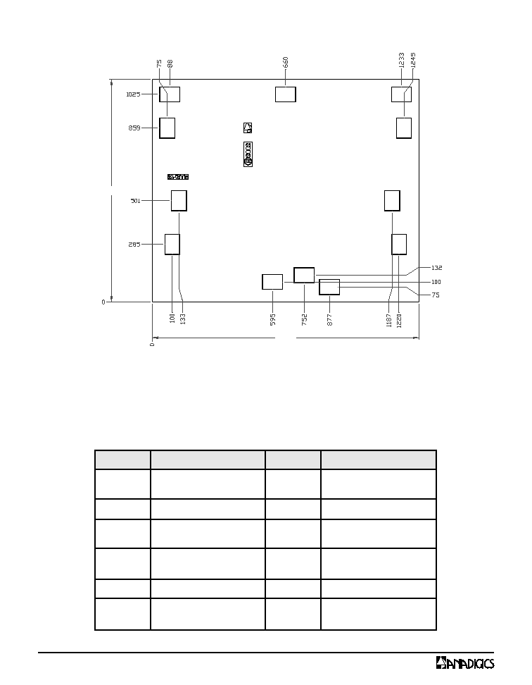
Figure 2: Die Configuration
Dimensions in
µ
m.
Bond Pads: 100
µ
m x 75
µ
m.
Die Thickness: 178
µ
m.
No backside metal.
Table 1: Pad Description
NAME
V1
RF1
RFG1
RFG2
RF2
V2
DESCRIPTION
Control voltage,
RF path 1
RF port, path 1
Ground
Ground
RF port, path 2
Control voltage,
RF path 2
NAME
RFG3
RF3
V3
VS2
RFC
VS1
DESCRIPTION
Ground
RF port, path 3
Control voltage,
RF path 3
Common port bias
voltage (logic high)
RF common port
Common port bias
voltage (logic high)
1320
1100
RF2G
RF2
V2
RF3G
RF3
V3
VS2
RFC
VS1
V1
RF1
RF1G

ADVANCED PRODUCT INFORMATION - Rev 0.2
04/2003
3
AWS5523
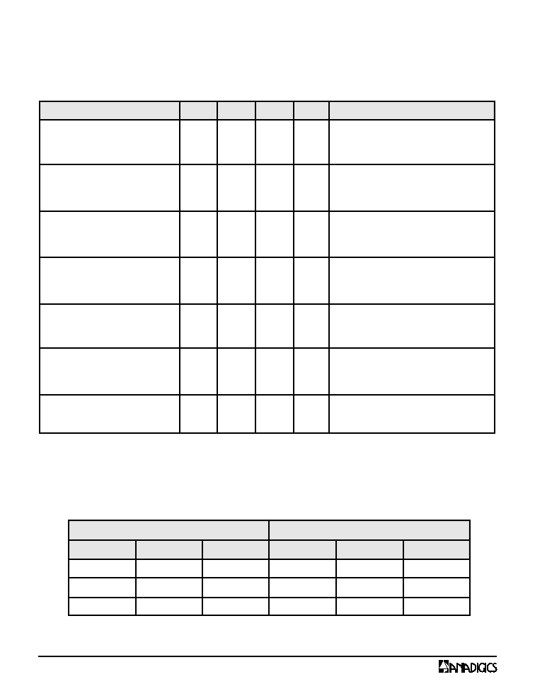
ELECTRICAL CHARACTERISTICS
Table 2: Absolute Minimum and Maximum Ratings
Stresses in excess of the absolute ratings may cause permanent damage. Functional operation is not
implied under these conditions. Exposure to absolute ratings for extended periods of time may adversely
affect reliability.
Notes:
(1) The VS1 and VS2 ports may remain open-circuited without damage to the device.
(2) Storage Temperature limits apply to the die only after it has been removed from the ANADIGICS
shipping material.
3. The RF1, RF2, RF3 and RFC ports should be AC-coupled. No external DC bias should be applied.
PARAMETER
Common Port Bias Voltage (V
S
)
Control Voltages (V
1
, V
2
, V
3
)
RF Input Power (P
IN
)
Storage Temperature
(2)
MIN
-0.2
-0.2
-
-65
MAX
+8.0
+8.0
10
+150
UNIT
V
V
W
∞
C
COMMENTS
at VS1 or VS2
(1)
at RF1, RF2, RF3
and RFC
The device may be operated safely over these conditions; however, parametric performance is guaranteed only
over the conditions defined in the electrical specifications.
Notes:
(1) For optimal linearity performance, the Common Port Bias Voltage (V
S
) should be set to the same Control Voltage used
to turn ON any of the individual RF paths. The VS1 and VS2 ports may remain open-circuited without damage to the
device, but with some degradation in linearity.
Table 3: Operating Ranges
PARAMETER
RF Frequency (f)
Common Port Bias Voltage (V
S
)
Control Voltages (V
1
, V
2
, V
3
)
Ambient Temperature (T
A
)
MIN
0.5
0
+2.5
-30
TYP
-
(1)
-
-
-
Max
2.5
+0.2
+3.5
+85
UNIT
GHz
V
∞
C
COMMENTS
applied at either VS1
or VS2 port
RF path OFF state
RF path ON state
4
ADVANCED PRODUCT INFORMATION - Rev 0.2
04/2003
AWS5523
Table 5: Switch Control Truth Table
CONTROL VOLTAGES
RF PATH SELECTION
V
1
+2.5 to +3.5 V
0 to +0.2 V
0 to +0.2 V
V
2
0 to +0.2 V
+2.5 to +3.5 V
0 to +0.2 V
V
3
0 to +0.2 V
0 to +0.2 V
+2.5 to +3.5 V
RFC - RF1
ON
OFF
OFF
RFC - RF2
OFF
ON
OFF
RFC - RF3
OFF
OFF
ON
Table 4: Electrical Specifications
(T
A
= +25
∞
C; RF ports terminated with 50
; V
n
= +2.7 V and is the Control Voltage for the ON path,
RFC-RFn; V
x
= 0 V and is the Control Voltage for the other two OFF paths, RFC-RFx)
Notes:
(1) Isolated RFx ports have a return loss of approximately -3 dB.
(2) For the Cellular Band, two tones with P
IN
= +22.5 dBm each, at 837 and 838 MHz. For the PCS Band, two tones with
P
IN
= +21 dBm each, at 1880 and 1881 MHz.
PARAMETER
Insertion Loss
1 GHz
2 GHz
Return Loss
(1)
1 GHz
2 GHz
Isolation
1 GHz
2 GHz
Input Third Order Intercept
(2)
800 MHz Cellular Band
1900 MHz PCS Band
2nd Harmonic Rejection
1 GHz
2 GHz
3rd Harmonic Rejection
1 GHz
2 GHz
Current Consumption
MIN
-
-
-
-
25
25
-
-
-
-
-
-
-
-
TYP
0.4
0.5
-29
-23
27
27
+66
+59
-77
-77
-72
-75
-
-
MAX
0.6
0.8
-20
-15
-
-
-
-
-65
-65
-65
-65
30
5
UNIT
dB
dB
dB
dBm
dBc
dBc
µ
A
COMMENTS
RFC port to selected RFn port
RFC port and selected RFn port
RFC port to isolated RFx ports
RFC port to selected RFn port
RFC port to selected RFn port
P
IN
= +34 dBm
P
IN
= +32 dBm
RFC port to selected RFn port
P
IN
= +34 dBm
P
IN
= +32 dBm
each Vn port
VS1 or VS2 port
ADVANCED PRODUCT INFORMATION - Rev 0.2
04/2003
5
AWS5523
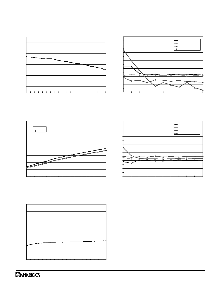
PERFORMANCE DATA
Figure 4: Harmonics of 1 GHz vs. Control Voltage
(ON path, V
x
= 0 V, f = 1 GHz, P
IN
= +34 dBm)
Figure 6: Harmonics of 2 GHz vs. Control Voltage
(ON path, V
x
= 0 V, f = 2 GHz, P
IN
= +32 dBm)
Figure 3: Insertion Loss vs. Frequency
(ON path, V
n
= +2.7 V, V
x
= 0 V)
Figure 5: Return Loss vs. Frequency
(ON path, V
n
= +2.7 V, V
x
= 0 V)
Figure 7: Isolation vs. Frequency
(OFF path, V
n
= +2.7 V, V
x
= 0 V)
-1.0
-0.8
-0.6
-0.4
-0.2
0.0
500
1000
1500
2000
2500
Frequency (MHz)
Insertion Loss (dB)
-40
-30
-20
-10
0
500
1000
1500
2000
2500
Frequency (MHz)
Return Loss (dB)
RFC port
RFn port
-40
-30
-20
-10
0
500
1000
1500
2000
2500
Frequency (MHz)
Isolation (dB)
-100
-90
-80
-70
-60
-50
-40
-30
2.5
2.6
2.7
2.8
2.9
3
3.1
3.2
3.3
3.4
3.5
Control Voltage (V)
Harmonic Level (dBc)
2nd Harmonic, Vs open
2nd Harmonic, Vs = Vn
3rd Harmonic, Vs open
3rd Harmonic, Vs = Vn
-100
-90
-80
-70
-60
-50
-40
-30
2.5
2.6
2.7
2.8
2.9
3
3.1
3.2
3.3
3.4
3.5
Control Voltage (V)
Harmonic Level (dBc)
2nd Harmonic, Vs open
2nd Harmonic, Vs = Vn
3rd Harmonic, Vs open
3rd Harmonic, Vs = Vn