 | –≠–ª–µ–∫—Ç—Ä–æ–Ω–Ω—ã–π –∫–æ–º–ø–æ–Ω–µ–Ω—Ç: ATA7609 | –°–∫–∞—á–∞—Ç—å:  PDF PDF  ZIP ZIP |

10/2002
V
BIAS
I
IN
V
REF
DC
Offset
Control
Low Pass
Filter
C
EXT
V
EE
V
OUT
V
OUT
ATA7609
10 Gb/s High Overload TIA
PRELIMINARY DATA SHEET - Rev 1.0
D1
Die
FEATURES
∑
1800
Differential Transimpedance
∑
3 mApp Maximum Input Current
∑
14 pA/
Hz Input Noise Current Density
∑
Single ≠5.2 V Power Supply
∑
Low Group Delay
∑
Outputs DC or AC Coupled
∑
Same Functionality as ATA7603 with the Output
Polarities Reversed
APPLICATIONS
∑
SONET/SDH OC-192 /STM-64 VSR,
Short-Reach, Intermediate-Reach, and
Long-Reach Receivers
∑
10 Gb/s Ethernet
∑
Fiber optic receivers, transceivers, and
transponders
PRODUCT DESCRIPTION
The ANADIGICS ATA7609 is a ≠5.2 V high-speed
transimpedance amplifier (TIA) designed for
10 Gb/s optical receiver applications available in
bare die form and manufactured using an InGaP
based HBT process. The device is used in
conjunction with a photodetector to convert an
optical signal into a differential output voltage that
can be AC or DC coupled to a post amplifier. The
ATA7609 has an internal overload support circuit
and can accept optical inputs as high as +3 dBm.
With its low noise and high optical overload capability,
the device is well suited for 10 Gb/s Ethernet and
OC-192 Very Short-Reach (VSR), Short-Reach,
Intermediate-Reach and Long-Reach optical
receivers, transceivers and transponders. The
ATA7609 is identical to the ATA7603 but with the
output polarities reversed.
Figure 1: Circuit Block Diagram
I
IN
V
OUT
C
EXT
V
EE
GND
GND
GND
GND
V
EE
V
OUT
GND

2
PRELIMINARY DATA SHEET - Rev 1.0
10/2002
ATA7609
286
m
m
170
m
m
140
m
m
303
m
m
I
IN
V
OUT
C
EXT
V
EE
GND
GND
GND
GND
ATA7609
Die Size: 1000 m x 910 m
m
m
Die Thickness: 178 m
Backside metal thickness: 5 m
m
m
Pad Opening: 100
m
m
m x 100 m
unless otherwise noted
Pad Pitch 150 m unless otherwise
noted
m
GND
286
m
m
V
EE
V
OUT
Figure 2: Die Size and Layout
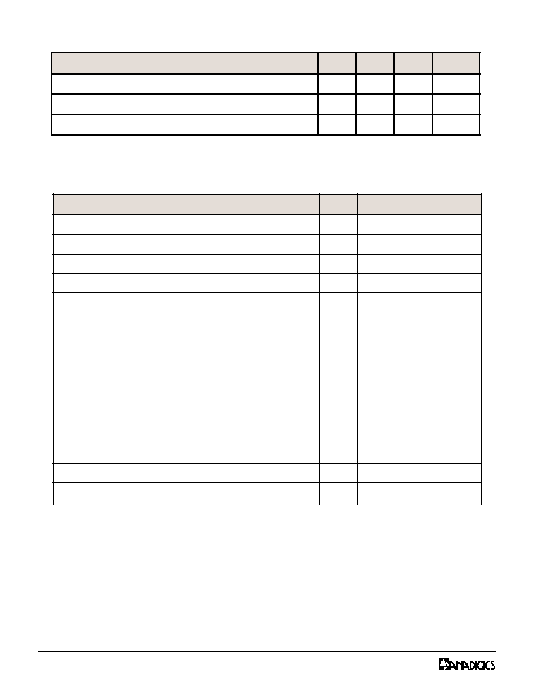
Table 1: Pad Description
D
A
P
N
O
I
T
P
I
R
C
S
E
D
S
T
N
E
M
M
O
C
V
E
E
e
g
a
tl
o
V
y
l
p
p
u
S
e
v
it
a
g
e
N
V
2
.
5
-
D
N
G
d
n
u
o
r
G
I
N
I
t
u
p
n
I
A
I
T
t
u
p
n
i
t
n
e
r
r
u
c
o
t
o
h
P
C
T
X
E
r
o
ti
c
a
p
a
C
l
a
n
r
e
t
x
E
n
a
r
o
f
n
o
it
c
e
n
n
o
C
ff
o
t
u
c
y
c
n
e
u
q
e
rf
w
o
l
e
h
t
s
t
e
S
V
T
U
O
e
g
a
tl
o
V
t
u
p
t
u
O
d
e
t
r
e
v
n
i-
n
o
N
t
u
p
n
i
l
a
c
it
p
o
h
ti
w
'
1
'
l
a
c
i
g
o
L
V
T
U
O
e
g
a
tl
o
V
t
u
p
t
u
O
d
e
t
r
e
v
n
I
t
u
p
n
i
l
a
c
it
p
o
h
ti
w
'
0
'
l
a
c
i
g
o
L

PRELIMINARY DATA SHEET - Rev 1.0
10/2002
ATA7609
3
ELECTRICAL CHARACTERISTICS
Table 2: Absolute Minimum and Maximum Ratings
Stresses in excess of the absolute ratings may cause permanent
damage. Functional operation is not implied under these conditions.
Exposure to absolute ratings for extended periods of time may
adversely affect reliability.
Table 3: Recommended Operating Conditions
The device may be operated safely over these conditions; however, parametric
performance is guaranteed only over the conditions defined in the electrical
specifications.
R
E
T
E
M
A
R
A
P
N
I
M
X
A
M
T
I
N
U
V
(
y
l
p
p
u
S
r
e
w
o
P
C
D
E
E
)
0
.
7
-
0
.
1
V
e
r
u
t
a
r
e
p
m
e
T
e
g
a
r
o
t
S
5
6
-
5
2
1
C
∞
t
n
e
r
r
u
C
t
u
p
n
I
C
D
-
0
.
5
A
m
)l
e
d
o
M
y
d
o
B
n
a
m
u
H
(
y
ti
v
it
i
s
n
e
S
D
S
E
0
0
1
-
V
R
E
T
E
M
A
R
A
P
N
I
M
P
Y
T
X
A
M
T
I
N
U
e
g
n
a
R
e
g
a
tl
o
V
g
n
it
a
r
e
p
O
0
5
.
5
-
2
.
5
-
0
9
.
4
-
V
e
g
n
a
R
e
r
u
t
a
r
e
p
m
e
T
g
n
it
a
r
e
p
O
)
1
(
0
4
-
-
5
8
o
C
e
r
u
t
a
r
e
p
m
e
T
h
c
a
tt
A
e
i
D
-
-
0
6
2
o
C
)
y
a
r
t
s
+
N
I
P
(
e
c
n
a
ti
c
a
p
a
C
e
d
o
i
d
o
t
o
h
P
-
5
2
2
.
0
3
.
0
F
p
y
ti
v
i
s
n
o
p
s
e
R
e
d
o
i
d
o
t
o
h
P
-
2
9
.
0
-
W
/
A
e
c
n
a
t
s
i
s
e
R
t
c
a
t
n
o
C
e
d
o
i
d
o
t
o
h
P
-
0
1
5
1
e
c
n
a
t
c
u
d
n
I
e
r
i
w
d
n
o
B
t
u
p
n
I
7
.
0
0
.
1
-
H
n
Notes:
(1) Defined at the interface between the die and the substrate.
4
PRELIMINARY DATA SHEET - Rev 1.0
10/2002
ATA7609
Table 4: DC Electrical Specifications
R
E
T
E
M
A
R
A
P
N
I
M
P
Y
T
X
A
M
T
I
N
U
)
s
t
u
p
t
u
O
d
e
l
p
u
o
C
C
D
(
t
n
e
r
r
u
C
y
l
p
p
u
S
-
5
9
0
2
1
A
m
e
g
a
tl
o
V
t
e
s
ff
O
t
u
p
n
I
-
7
.
3
-
-
V
)
s
t
r
o
p
h
t
o
b
(
e
g
a
tl
o
V
t
e
s
ff
O
t
u
p
t
u
O
-
2
.
0
-
-
V
Table 5: AC Electrical Specifications
(1)
(V
EE
= -5.5 V to -4.9 V, Operating Temperature = -40 ∞C to + 85 ∞C unless otherwise noted)
R
E
T
E
M
A
R
A
P
N
I
M
P
Y
T
X
A
M
T
I
N
U
R
(
e
c
n
a
d
e
p
m
i
s
n
a
r
T
l
a
it
n
e
r
e
f
f
i
D
l
a
n
g
i
S
ll
a
m
S
L =
0
0
1
)
0
0
3
1
0
0
8
1
-
R
(
e
c
n
a
d
e
p
m
i
s
n
a
r
T
l
a
it
n
e
r
e
f
f
i
D
l
a
n
g
i
S
ll
a
m
S
L =
0
0
1
)
)
2
(
0
0
4
1
-
-
h
t
d
i
w
d
n
a
B
l
a
n
g
i
S
ll
a
m
S
5
.
8
5
.
9
-
z
H
G
f
f
o
t
u
C
y
c
n
e
u
q
e
r
F
w
o
L
)
3
(
-
0
3
-
z
H
k
g
n
i
k
a
e
P
-
-
5
.
1
B
d
)
z
H
G
0
.
8
o
t
z
H
M
0
0
5
(
n
o
it
a
i
v
e
D
y
a
l
e
D
p
u
o
r
G
)
4
(
-
0
3
-
s
p
)
z
H
G
5
.
9
o
t
z
H
G
8
(
n
o
it
a
i
v
e
D
y
a
l
e
D
p
u
o
r
G
)
4
(
-
0
4
-
s
p
t
n
e
r
r
u
C
t
u
p
n
I
m
u
m
i
x
a
M
-
-
0
.
3
p
p
A
m
d
a
o
l
r
e
v
O
l
a
c
it
p
O
)
5
(
-
3
+
-
m
B
d
t
n
e
r
r
u
C
e
s
i
o
N
S
M
R
d
e
r
r
e
f
e
R
t
u
p
n
I
)
6
(
-
4
.
1
-
µA
y
t
i
s
n
e
D
t
n
e
r
r
u
C
e
s
i
o
N
d
e
r
r
e
f
e
R
t
u
p
n
I
e
g
a
r
e
v
A
)
6
(
-
4
1
0
2
/
A
p
z
H
y
t
i
v
it
i
s
n
e
S
l
a
c
it
p
O
)
5
(
-
9
1
-
-
m
B
d
g
n
i
w
S
e
g
a
tl
o
V
t
u
p
t
u
O
d
e
d
n
e
-
e
l
g
n
i
S
m
u
m
i
x
a
M
-
0
0
4
0
5
5
p
p
V
m
)
z
H
G
8
o
t
z
H
M
0
1
(
s
s
o
L
n
r
u
t
e
R
t
u
p
t
u
O
-
-
0
1
-
B
d
)
z
H
G
0
2
o
t
z
H
M
8
(
s
s
o
L
n
r
u
t
e
R
t
u
p
t
u
O
-
-
5
-
B
d
Notes:
(1) The specifications are based upon the use of a PIN photodiode with a responsivity of 0.92 A/W and a
capacitance of C
DIODE
+ C
STRAY
= 0.3 pF max connected to I
IN
via a 1.0 nH bond wire.
(2) Operating temperature range = -5 ∞C to +85 ∞C.
(3) With the use of an external 10 nF capacitor.
(4) Maximum value - minimum value
(5) Measured at 10
-10
BER with a 2
23
-1 PRBS at 10 Gb/s
(6) Bandwidth = 9 GHz
PRELIMINARY DATA SHEET - Rev 1.0
10/2002
ATA7609
5
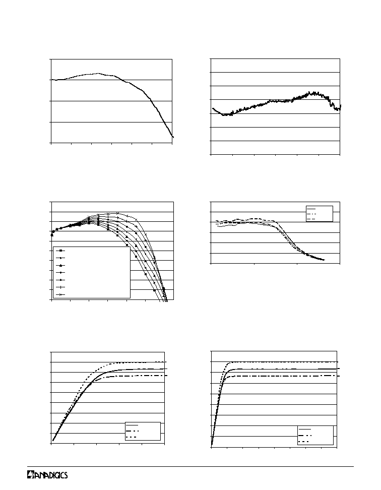
PERFORMANCE DATA
3 dB Bandwidth = 9.9 GHz
15.2
18.2
21.2
24.2
27.2
0
2
4
6
8
10
12
Frequency(GHz)
R
esponse(
dB
)
Figure 3: Typical Small Signal Frequency
Response
Figure 4: Typical Small Signal Group Delay
180
200
220
240
260
280
300
320
0
2
4
6
8
10
12
Frequency(GHz)
Gr
oup
Delay
(
ps)
55
56
57
58
59
60
61
62
63
64
65
0
2
4
6
8
10
12
Frequency (GHz)
Gain
(dB)
Lin = 30mils, BW = 9.3GHz
Lin = 35mils, BW = 9.6GHz
Lin = 40mils, BW = 9.9GHz
Lin = 45mils, BW = 10.6GHz
Lin = 50mils, BW = 10.9GHz
Lin = 55mils, BW = 11.1GHz
Lin = 60mils, BW = 11.1GHz
Figure 5: Bandwidth vs. Input Inductance
Figure 6: Differential Transimpedance vs.
Input Current
0.000
0.500
1.000
1.500
2.000
2.500
3.000
10
100
1000
10000
Input Current (uApp)
Tz
(
K
ohm
s
)
Vee=-5.2V
VEE=-4.9V
VEE=-5.5V
0
100
200
300
400
500
600
700
800
900
0
200
400
600
800
1000
Input Current (uApp)
Output
V
o
ltage
(
mVpp)
VEE=-5.2V
VEE=-4.9V
VEE=-5.5V
Figure 7: Differential Output Voltage vs.
Input Current up to 1000 App
m
0
100
200
300
400
500
600
700
800
900
0
500
1000
1500
2000
2500
3000
3500
4000
Input Current (uApp)
O
u
t
put
V
o
l
t
age
(
m
V
pp)
VEE=-5.2V
VEE=-4.9V
VEE=-5.5V
Figure 8: Differential Output Voltage vs.
Input Current up to 4000 App
m