08/2001
ARA3000
Address-Programmable Telephony
Reverse Amplifier with Step Attenuator
PRELIMINARY DATA SHEET - Rev 1.1
FEATURES
∑ Low cost integrated amplifier with step
attenuator
∑ Attenuation Range: 0-56 dB, adjustable in 2 dB
increments via a 3 wire serial control
∑ Meets DOCSIS distortion requirements at a
+60dBmV output signal level
∑ Programmable address allows multiple parts
to share control bus
∑ Programmable 2 bit data port output
∑ Low distortion and low noise
∑ Frequency range: 5-100 MHz
∑ 5 Volt operation
∑ -40 to +85
o
C temperature range
APPLICATIONS
∑ DOCSIS Compliant IP Telephony Systems
∑ CATV Interactive Set-Top Box
∑ OpenCable Set-Top Box
∑ Residential Gateway
The ARA3000 is designed to provide additional
reverse path amplification and isolation in IP
Telephony systems. It incorporates a digitally
controlled precision step attenuator, followed by a
single-stage output amplifier that exceeds DOCSIS
distortion and noise requirements at a +60dBmV
output level while only requiring a single polarity +5V
supply. The precision attenuator can handle input
powers up to +58 dBmV, and provides up to 56 dB of
attenuation in 2 dB increments. The output amplifier
stage can be shut down and bypassed by a low
insertion loss switch on-chip to save power. The
ARA3000 has a programmable address that allows
multiple devices to share a common control bus,
and a 2-bit data port for control of external devices.
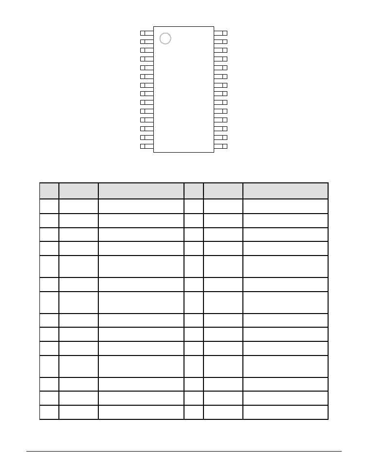
The ARA3000 is offered in a 28-pin SSOP package
featuring an exposed paddle on the bottom of the
package.
PRODUCT DESCRIPTION
Figure 1. Functional Block Diagram
S23 Package
28 Pin SSOP
with Exposed Paddle
Serial to Parallel
Interface
5 Bit Attenutor
32 / 16 / 8 / 4 / 2dB
2
Data Port
D[1:0]
ATTN
IN
CLK
EN
DAT
Address
C[1:0]
V
CTRL
AMP
OUT
Bypass
2

PRELIMINARY DATA SHEET - Rev 1.1
08/2001
3
ARA3000
ELECTRICAL CHARACTERISTICS
R
E
T
E
M
A
R
A
P
N
I
M
X
A
M
T
I
N
U
)
3
2
,
0
1
s
n
i
p
(
y
l
p
p
u
S
g
o
l
a
n
A
0
9
C
D
V
V
:
y
l
p
p
u
S
l
a
ti
g
i
D
CMOS
)
1
1
n
i
p
(
0
6
C
D
V
V
:l
o
rt
n
o
C
r
e
if
il
p
m
A
CTRL
)
1
2
n
i
p
(
5
-
6
V
F
R
t
u
p
n
I
t
a
r
e
w
o
P
)
9
n
i
p
(
-
8
5
V
m
B
d
)
6
1
,
5
1
,
4
1
,
3
1
,
2
1
s
n
i
p
(
e
c
a
fr
e
t
n
I
l
a
ti
g
i
D
5
.
0
-
V
CMOS
5
.
0
+
V
e
r
u
t
a
r
e
p
m
e
T
e
g
a
r
o
t
S
5
5
-
0
0
2
+
o
C
e
r
u
t
a
r
e
p
m
e
T
g
n
ir
e
d
l
o
S
-
0
6
2
o
C
e
m
i
T
g
n
ir
e
d
l
o
S
-
5
c
e
S
Table 2: Absolute Minimum and Maximum Ratings
Table 3: Operating Ranges
R
E
T
E
M
A
R
A
P
N
I
M
P
Y
T
X
A
M
T
I
N
U
V
:
y
l
p
p
u
S
g
o
l
a
n
A
DD
)
3
2
,
0
1
s
n
i
p
(
5
.
4
5
7
C
D
V
V
:
y
l
p
p
u
S
l
a
ti
g
i
D
CMOS
)
1
1
n
i
p
(
0
.
3
-
5
.
5
C
D
V
)
6
1
,
5
1
,
4
1
,
3
1
,
2
1
s
n
i
p
(
e
c
a
fr
e
t
n
I
l
a
ti
g
i
D
0
-
V
CMOS
V
V
:l
o
rt
n
o
C
r
e
if
il
p
m
A
CTRL
)
1
2
n
i
p
(
0
3
5
.
5
V
e
r
u
t
a
r
e
p
m
e
T
e
s
a
C
0
4
-
5
2
5
8
o
C
Stresses in excess of the absolute ratings may cause permanent damage. Functional
operation is not implied under these conditions. Exposure to absolute ratings for
extended periods of time may adversely affect reliability.
The device may be operated safely over these conditions; however, parametric
performance is guaranteed only over the conditions defined in the electrical specifications.
Notes:
1. Pins 2, 9 and 27 should be AC-coupled. No external DC bias should be applied.
2. Pin 1 should be pulled to ground through a resistor. No external DC bias should be
applied.
3. Pins 4, 5, 6, 7, 8, 22 and 26 should be AC-grounded. No external DC bias should be
applied.

4
PRELIMINARY DATA SHEET - Rev 1.1
08/2001
ARA3000
R
E
T
E
M
A
R
A
P
N
I
M
P
Y
T
X
A
M
T
I
N
U
S
T
N
E
M
M
O
C
)
3
2
,
0
1
s
n
i
p
(
t
n
e
rr
u
C
y
l
p
p
u
S
g
o
l
a
n
A
-
-
0
2
1
2
1
-
-
A
m
d
e
l
b
a
n
e
r
e
if
il
p
m
A
d
e
s
s
a
p
y
b
r
e
if
il
p
m
A
)
1
1
n
i
p
(
t
n
e
rr
u
C
y
l
p
p
u
S
l
a
ti
g
i
D
S
O
M
C
-
2
-
A
m
g
n
it
t
e
s
n
o
it
a
u
n
e
tt
a
x
a
M
n
o
it
p
m
u
s
n
o
C
r
e
w
o
P
l
a
t
o
T
-
-
0
1
6
0
7
-
-
W
m
W
m
d
e
l
b
a
n
e
r
e
if
il
p
m
A
d
e
s
s
a
p
y
b
r
e
if
il
p
m
A
Note: As measured in ANADIGICS test fixture
Table 4: DC Electrical Specifications
T
A
=25
∞
C; V
DD
, V
CMOS
= +5.0 VDC; V
CTRL
= +5.0 V (Amp enabled); V
CTRL
= 0 V (Amp bypassed)
R
E
T
E
M
A
R
A
P
N
I
M
P
Y
T
X
A
M
T
I
N
U
S
T
N
E
M
M
O
C
n
i
a
G
4
1
6
1
-
B
d
,
g
n
it
t
e
s
n
o
it
a
u
n
e
tt
a
B
d
0
d
e
l
b
a
n
e
r
e
if
il
p
m
a
5
.
2
-
7
.
1
-
-
B
d
,
g
n
it
t
e
s
n
o
it
a
u
n
e
tt
a
B
d
0
d
e
s
s
a
p
y
b
r
e
if
il
p
m
a
s
s
e
n
t
a
l
F
n
i
a
G
-
5
.
0
-
B
d
z
H
M
2
4
o
t
5
e
r
u
t
a
r
e
p
m
e
T
r
e
v
o
n
o
it
a
ir
a
V
n
i
a
G
-
6
0
0
.
0
-
-
C
∞
/
B
d
s
p
e
t
S
n
o
it
a
u
n
e
tt
A
B
d
2
B
d
4
B
d
8
B
d
6
1
B
d
2
3
4
5
.
1
6
.
3
7
.
7
5
.
5
1
2
.
0
3
5
7
.
1
9
.
3
1
.
8
9
.
5
1
7
.
0
3
0
.
2
2
.
4
3
.
8
3
.
6
1
2
.
1
3
B
d
c
i
n
o
t
o
n
o
M
n
o
it
a
l
o
s
I
m
u
m
i
x
a
M
-
0
6
-
B
d
,
g
n
it
t
e
s
n
o
it
u
n
e
tt
a
B
d
2
6
d
e
l
b
a
s
i
d
r
e
if
il
p
m
a
2
d
n
l
e
v
e
L
n
o
it
r
o
t
s
i
D
c
i
n
o
m
r
a
H
-
5
5
-
8
4
-
c
B
d
P
OUT
5
7
o
t
n
i
V
m
B
d
0
6
+
=
d
e
l
b
a
n
e
r
e
if
il
p
m
a
,
s
m
h
O
-
0
6
-
8
4
-
c
B
d
P
IN
5
7
m
o
rf
V
m
B
d
8
5
+
=
d
e
s
s
a
p
y
b
r
e
if
il
p
m
a
,
s
m
h
O
3
d
r
l
e
v
e
L
n
o
it
r
o
t
s
i
D
c
i
n
o
m
r
a
H
-
0
6
-
8
4
-
c
B
d
P
OUT
5
7
o
t
n
i
V
m
B
d
0
6
+
=
d
e
l
b
a
n
e
r
e
if
il
p
m
a
,
s
m
h
O
-
0
6
-
8
4
-
c
B
d
P
IN
5
7
m
o
rf
V
m
B
d
8
5
+
=
d
e
s
s
a
p
y
b
r
e
if
il
p
m
a
,
s
m
h
O
Table 5: AC Electrical Specifications
T
A
=25
∞
C; V
DD
, V
CMOS
= +5.0 VDC; V
CTRL
= +5.0 V (Amp enabled); V
CTRL
= 0 V (Amp bypassed)