
08/2001
S3 Package
Modified 16 Pin SOIC
ADC20013
950-2050 MHz DBS Tuner IC
Data Sheet - Rev 2.9
Figure 1: Functional Block Diagram
FEATURES
∑
Monolithic DBS Tuner IC
∑
On Chip Oscillator
∑
6 dB Noise Figure
∑
11 dB Conversion Gain
∑
Single + 5V Supply
∑
Small Size
∑
Low Cost
∑
High Reliability
∑
Surface Mount Package
PRODUCT DESCRIPTION
The ANADIGICS DBS (Direct Broadcast Satellite)
Tuner IC is intended for use in high volume, low cost
manufacturing of compact DBS tuners for satellite
receivers and integrated satellite ready TV/VTR
receivers.
The ADC20013 Tuner IC provides DBS tuner
manufacturers the ability to produce, in high volumes,
tuners with low component count, minimal tuning,
small size, high reliability and exceptional price-
performance ratios. The ADC20013 offers a high
degree of functionality in a very small and user friendly
configuration.
LO
IF
OSC
RF
DD
V

ADC20013
2
Data Sheet - Rev 2.9
08/2001
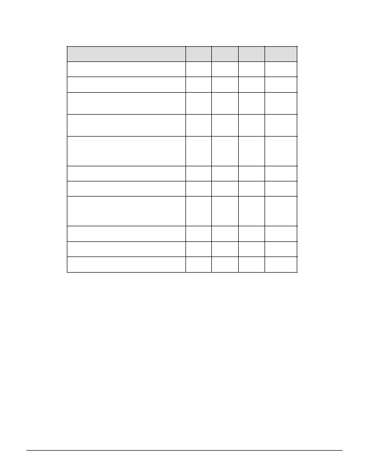
Table 1: Absolute Minimum and Maximum Ratings
ELECTRICAL CHARACTERISTICS
Stresses in excess of the absolute ratings may cause permanent
damage. Functional operation is not implied under these conditions.
Exposure to absolute ratings for extended periods of time may
adversely affect reliability.
Table 2: Operating Ranges
The device may be operated safely over these conditions; however, parametric
performance is guaranteed only over the conditions defined in the electrical
specifications.
R
E
T
E
M
A
R
A
P
N
I
M
P
Y
T
X
A
M
T
I
N
U
y
c
n
e
u
q
e
r
F
F
R
O
L
F
I
0
5
9
0
3
4
1
-
-
-
0
8
4
0
5
0
2
0
3
5
2
-
z
H
M
z
H
M
z
H
M
V
D
D
-
5
+
-
C
D
V
e
r
u
t
a
r
e
p
m
e
T
e
s
a
C
5
5
-
-
5
8
+
O
C
R
E
T
E
M
A
R
A
P
N
I
M
X
A
M
T
I
N
U
V
D
D
V
/
F
I
0
7
+
C
D
V
V
O
L
5
-
5
.
0
+
C
D
V
V
F
R
0
1
-
5
.
0
+
C
D
V
V
C
S
O
5
-
5
.
0
+
C
D
V
e
r
u
t
a
r
e
p
m
e
T
e
g
a
r
o
t
S
5
5
-
0
0
1
+
C
∞
F
R
r
e
w
o
P
t
u
p
n
I
0
1
+
m
B
d
O
L
r
e
w
o
P
t
u
p
n
I
7
1
+
m
B
d
ADC20013
Data Sheet - Rev 2.9
08/2001
3
Table 3: Electrical Specifications
(T
A
= 25
o
C; V
DD
= + 5V)
Notes:
(1) Measured in ANADIGICS test fixture with Toshiba 1SV186 off-chip-varactor.
(2) Includes external coupling through test fixture.
(3) Oscillator output for external PLL. (Pin 14)
(4) Measured at 1450 & 1750 MHz.
(5) Measured using PLL (LBW =1KHz, Reference = 1.25 MHz, Step Size = 10 MHz).
(6) Measured in ANADIGICS test setup.
(7) See Smith charts.
R
E
T
E
M
A
R
A
P
N
I
M
P
Y
T
X
A
M
T
I
N
U
n
i
a
G
n
o
i
s
r
e
v
n
o
C
)
6
(
6
1
1
-
B
d
e
r
u
g
i
F
e
s
i
o
N
B
S
S
)
6
(
-
5
.
6
1
1
B
d
D
M
I
r
e
d
r
O
d
ri
h
T
)
4
(
)t
r
a
p
A
z
H
M
5
,
s
e
n
o
T
m
B
d
0
2
-
(
-
0
4
-
5
3
-
c
B
d
D
M
I
r
e
d
r
O
d
n
o
c
e
S
)l
e
v
e
L
t
u
p
n
I
m
B
d
0
2
-
(
-
5
2
-
0
2
-
c
B
d
e
g
a
k
a
e
L
O
L
)
2
(,
)
1
(
tr
o
P
F
R
tr
o
P
F
I
-
-
0
3
-
0
5
2
-
3
m
B
d
m
B
d
L
L
P
r
o
f
l
e
v
e
L
t
u
p
t
u
O
O
L
)
3
(
8
-
4
-
-
m
B
d
e
g
a
tl
o
V
g
n
i
n
u
T
)
1
(
)
T
V
(
1
-
0
2
s
tl
o
V
e
s
i
o
N
e
s
a
h
P
O
C
V
)
5
(
t
e
s
ff
O
z
H
k
0
1
t
e
s
ff
O
z
H
k
0
0
1
-
-
0
7
-
0
0
1
-
5
6
-
5
9
-
z
H
/
c
B
d
z
H
/
c
B
d
e
c
n
a
d
e
p
m
I
t
u
p
n
I
)
7
(
-
-
-
-
e
c
n
a
d
e
p
m
I
t
u
p
t
u
O
)
7
(
-
-
-
-
t
n
e
r
r
u
C
y
l
p
p
u
S
r
e
w
o
P
-
0
6
5
8
A
m

ADC20013
4
Data Sheet - Rev 2.9
08/2001
Figure 2: Test Circuit
ADC20013
Data Sheet - Rev 2.9
08/2001
5
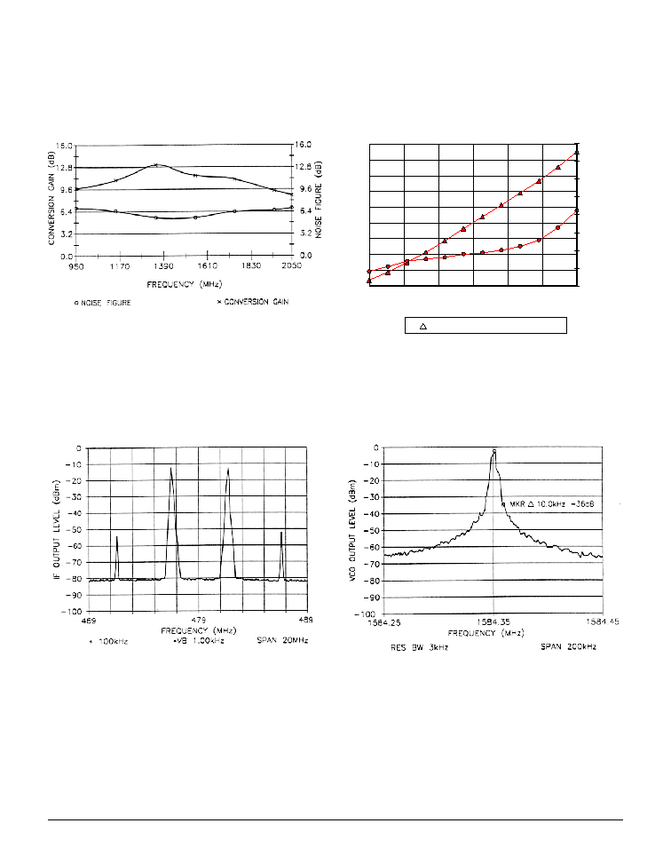
PERFORMANCE DATA
Figure 3: Conversion Gain and Noise
Figure vs Frequency
Figure 4: Oscillator Tuning Curve
Figure 5: Third Order IMD
RF Input Power Level -20dBm/Tone
Figure 6: VCO Phase Noise
1400
1600
1800
2000
2200
2400
2600
0
2
4
6
8
10
12
14
16
18
0
0.1
0.2
0.3
0.4
0.5
0.6
0.7
0.8
S
T
ANDARD DE
V
I
AT
I
O
N
VARACTOR VOLTAGE STD
V
ARACT
O
R
V
O
L
T
A
G
E
(V
d
c
)
OSCILLATOR FREQUENCY (MHz)