
05/200
5
ACD0900
VHF/UHF CATV/TV Tuner
Downconverter
Data Sheet - Rev 2.2
Figure 1: Functional Block Diagram
FEATURES
∑
Integrated Monolithic Downconverter
∑
8 dB Noise Figure
∑
10 dB Conversion Gain
∑
High Linearity
∑
Small Size
∑
Low Cost
∑
High Reliability
∑
RoHS-Compliant Package Option
S3 Package
Modified 16 Pin SOIC
PRODUCT DESCRIPTION
The ACD0900 MMIC is a high performance
downconverter fabricated entirely in GaAs. It is
designed for use as the second conversion stage
in double-conversion tuners and cable modems,
downconverting 900 -1200 MHz RF inputs to a fixed
IF of 35 - 150 MHz (depending on LO frequency).
The IC incorporates a low noise amplifier, high
linearity double balanced mixer, phase splitter and
oscillator in a modified SOIC 16 lead surface mount
package. The high degree of functionality allows
tuner manufactures to reduce size and cost by
lowering the component count and decreasing the
amount of production alignment steps, while
significantly improving performance and reliability.
PHASE
8
5
6
7
SPLITTER
OSC
2
3
4
1
MXR
9
12
11
10
15
14
13
16
LOW NOISE
AMP.
IF
1,
+5V
GND
N/C
GND
RF
IN
I
SET
GND
N/C
+5V
T
CKT
GND
OSC
OUT
GND
IF
2,
+ 5V

2
Data Sheet - Rev 2.2
05/2005
ACD0900
* Do not connect pin 9 to GND
Table 1: Pin Description
N
I
P
N
O
I
T
P
I
R
C
S
E
D
N
I
P
N
O
I
T
P
I
R
C
S
E
D
1
F
I
1
V
,
F
I
D
D
9
*
C
N
2
D
N
G
0
1
V
O
L
D
D
3
C
N
1
1
T
T
K
C
4
D
N
G
2
1
D
N
G
5
D
N
G
3
1
D
N
G
6
F
R
N
I
4
1
T
U
O
C
S
O
7
I
T
E
S
5
1
D
N
G
8
D
N
G
6
1
F
I
2
V
,
F
I
D
D
Data Sheet - Rev 2.2
05/2005
3
ACD0900
ELECTRICAL CHARACTERISTICS
Table 2: Absolute Minimum and Maximum Ratings
Note:
(1) V
TCKT
: Maximum voltage that may be applied to pin 11 of the device without
damaging the IC. DC blocking capacitor (1500 pF) between pin 11 and the
external tuning circuit is mandatory.
Stresses in excess of the absolute ratings may cause permanent
damage. Functional operation is not implied under these conditions.
Exposure to absolute ratings for extended periods of time may
adversely affect reliability.
Table 3: Operating Ranges
The device may be operated safely over these conditions; however, parametric
performance is guaranteed only over the conditions defined in the electrical
specifications.
R
E
T
E
M
A
R
A
P
N
I
M
X
A
M
T
I
N
U
V
F
I
D
D
V
,
O
L
D
D
V
,
C
S
O
-
9
s
tl
o
V
V
F
R
V
,
T
K
C
T
)
1
(
-
0
s
tl
o
V
e
r
u
t
a
r
e
p
m
e
T
e
g
a
r
o
t
S
5
5
-
0
0
2
C
∞
e
r
u
t
a
r
e
p
m
e
T
g
n
ir
e
d
l
o
S
-
0
6
2
C
∞
e
m
i
T
g
n
ir
e
d
l
o
S
-
5
.
c
e
S
r
e
w
o
P
t
u
p
n
I
F
R
-
0
1
+
m
B
d
r
e
w
o
P
t
u
p
n
I
O
L
-
7
1
+
m
B
d
e
c
n
a
t
s
i
s
e
R
l
a
m
r
e
h
T
-
5
2
W
/
C
∞
R
E
T
E
M
A
R
A
P
N
I
M
P
Y
T
X
A
M
T
I
N
U
y
c
n
e
u
q
e
r
F
F
R
O
L
F
I
0
0
9
5
3
9
5
3
-
-
-
0
0
2
1
0
5
3
1
0
5
1
z
H
M
V
F
I
D
D
V
,
O
L
D
D
5
7
.
4
0
.
5
5
2
.
5
C
D
V
e
r
u
t
a
r
e
p
m
e
T
e
s
a
C
5
5
-
-
5
8
C
∞

4
Data Sheet - Rev 2.2
05/2005
ACD0900
Table 4: Electrical Specifications
( T
A
= +25
∞
C; V
DDIF
, V
DDLO
= +5V)
Notes:
(1) Combined output ( IF
1
+ IF
2
) using a balun. NOTE: Gain at either port (uncombined), with unused port
terminated in 50 W, is 3 dB lower
(2) Two tones @ -15 dBm per tone
R
E
T
E
M
A
R
A
P
N
I
M
P
Y
T
X
A
M
T
I
N
U
S
T
N
E
M
M
O
C
s
e
i
c
n
e
u
q
e
r
F
F
R
O
L
F
I
-
-
-
0
7
1
1
5
4
2
1
5
7
-
-
-
z
H
M
t
e
s
f
f
O
z
H
K
0
1
@
e
s
i
o
N
e
s
a
h
P
-
9
8
-
5
.
5
8
-
z
H
/
c
B
d
e
r
u
g
i
F
e
s
i
o
N
-
0
.
8
5
.
9
B
d
)
d
a
o
L
0
0
2
(
n
i
a
G
)
1
(
8
.
7
5
.
9
-
B
d
)
d
a
o
L
0
0
2
(
D
M
I
r
e
d
r
O
d
r
3
)
2
(
-
9
5
-
4
5
-
c
B
d
)
d
a
o
L
0
0
2
(
P
I
t
u
p
n
I
r
e
d
r
O
d
r
3
)
2
(
2
1
+
-
-
m
B
d
,
z
H
K
5
1
@
n
o
i
t
a
l
u
d
o
M
s
s
o
r
C
)
2
(
n
o
i
t
a
l
u
d
o
M
M
A
%
9
9
-
6
5
-
-
c
B
d
n
o
i
t
p
m
u
s
n
o
C
t
n
e
r
r
u
C
-
0
8
0
1
1
A
m
V
0
.
5
@
n
o
i
t
p
m
u
s
n
o
C
r
e
w
o
P
-
0
0
4
-
W
m

Data Sheet - Rev 2.2
05/2005
5
ACD0900
Figure 2: Test Circuit Schematic
1
2
4
5
9
8
7
6
3
10
16
15
14
13
12
11
PHASE
SPLITTER
LOW
NOISE
AMP
OSC
5.6
0.001
µ
F
RF
IN
NC
IF
1
IF
2
0.001
µ
F
OSC Output
to Prescalar
+5V
IF
OUT
3.3 pF
2 K
1SV245
L
12 K
0.01
µ
F
Vtune
0.01
µ
F
0.1
µ
F
+5V
330
µ
F
100 pF
MIXER
NC
N:1
6
Data Sheet - Rev 2.2
05/2005
ACD0900
PERFORMANCE DATA
MEASURED IN 50
SYSTEM
IMPEDANCE REFERENCE PLANE AT PIN 16
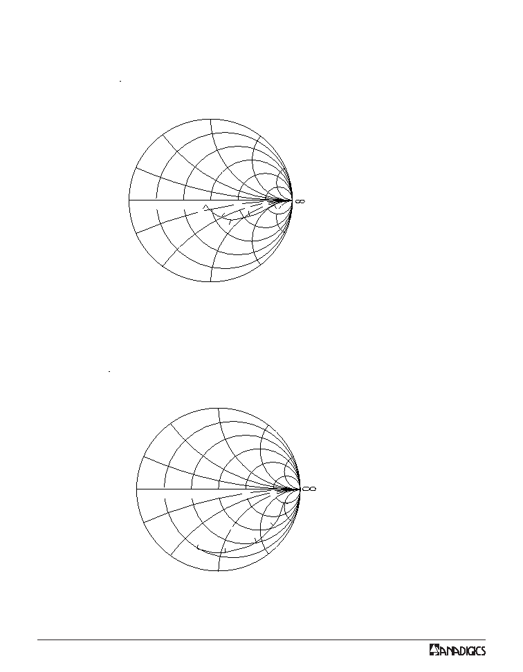
.5
5
2
.2
.2
0
-.2
-.5
-1
-2
-5
5
2
1
.5
1
1
2
4
3
5
1:
50 MHz
251.64
- 222.35 j
2:
150 MHz
60.89
-144.22 j
3:
250 MHz
26.32
- 89.16 j
4:
400 MHz
13.24
- 49.55 j
5 :
500 MHz
10.08
- 34.10 j
START: 50 MHz
STOP: 500 MHz
Figure 4: IF Output Impedance
2000MHz
50MHz
. 2
.2
5
2
1
.5
IMPEDANCE REFERENCE PLANE AT PIN 6
MEASURED IN 50
SYSTEM
START:
STOP:
1:
50 MHz
183.00
- 21.75 j
2:
250 MHz
135.48
-58.21 j
3:
750 MHz
75.92
- 43.12 j
4:
1000 MHz
64.93
- 32.29 j
5 :
2000 MHz
43.79
-4.71 j
0
-.2
-.5
-.1
- 2
- 5
.5
1
2
5
1
2
3
4
5
Figure 3: RF Input Impedance

Data Sheet - Rev 2.2
05/2005
7
ACD0900
-5.8
MEASURED IN 50
SYSTEM
IMPEDANCE REFERENCE PLANE AT PIN 11
-1
.5
5
2
1
.2
-.17
-.2
-.5
-2
-5
5
4
3
2
1
START: 50 MHz
STOP:
2000 MHz
1:
50 MHz
259.67
- 1200 j
2:
612 MHz
- 20.97
- 50.63 j
3:
1000 MHz
- 9.28
- 14.88 j
4:
1500 MHz
- 5.36
7.99 j
5 :
2000 MHz
0.64
27.12 j
Figure 5: LO Impedance
8
Data Sheet - Rev 2.2
05/2005
ACD0900
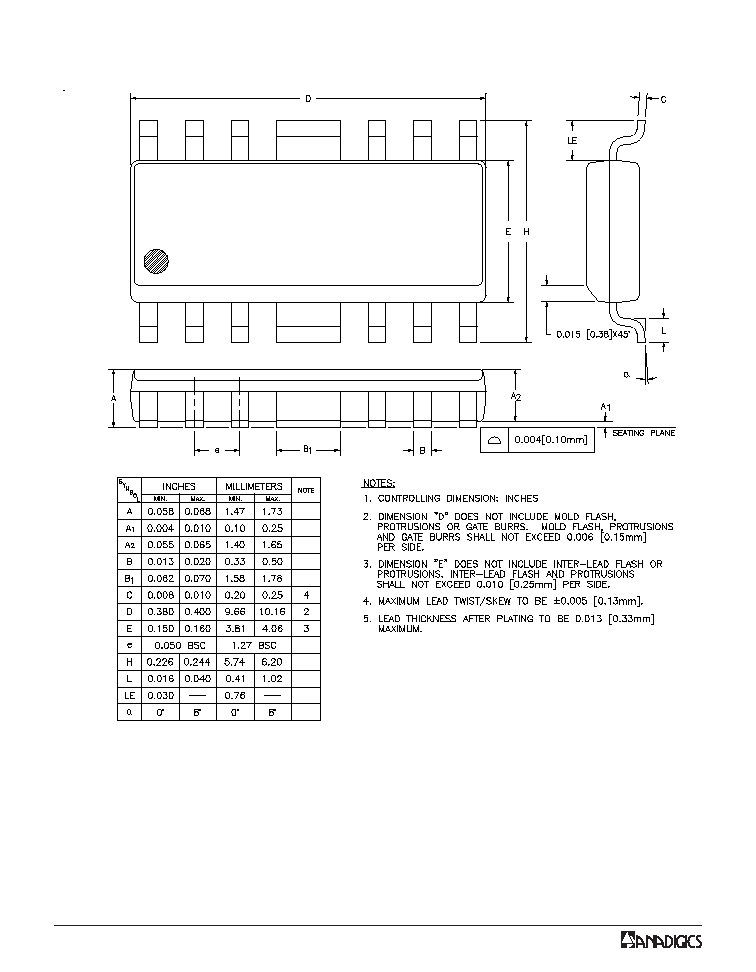
PACKAGE OUTLINE
Figure 6: S3 Package Outline - Modified 16 Pin SOIC

Data Sheet - Rev 2.2
05/2005
9
ACD0900
NOTES

10
Data Sheet - Rev 2.2
05/2005
ACD0900
NOTES

Data Sheet - Rev 2.2
05/2005
11
ACD0900
NOTES

WARNING
ANADIGICS products are not intended for use in life support appliances, devices or systems. Use of an ANADIGICS
product in any such application without written consent is prohibited.
IMPORTANT NOTICE
ANADIGICS, Inc.
141 Mount Bethel Road
Warren, New Jersey 07059, U.S.A.
Tel: +1 (908) 668-5000
Fax: +1 (908) 668-5132
URL: http://www.anadigics.com
E-mail: Mktg@anadigics.com
ANADIGICS, Inc. reserves the right to make changes to its products or to discontinue any product at any time without
notice. The product specifications contained in Advanced Product Information sheets and Preliminary Data Sheets are
subject to change prior to a product's formal introduction. Information in Data Sheets have been carefully checked and are
assumed to be reliable; however, ANADIGICS assumes no responsibilities for inaccuracies. ANADIGICS strongly urges
customers to verify that the information they are using is current before placing orders.
Data Sheet - Rev 2.2
05/2005
12
ACD0900
ORDERING INFORMATION
R
E
B
M
U
N
R
E
D
R
O
E
R
U
T
A
R
E
P
M
E
T
E
G
N
A
R
E
G
A
K
C
A
P
N
O
I
T
P
I
R
C
S
E
D
G
N
I
G
A
K
C
A
P
T
N
E
N
O
P
M
O
C
R
T
C
3
S
0
0
9
0
D
C
A
C
∞
5
8
+
o
t
C
∞
5
5
-
C
I
O
S
n
i
P
6
1
d
e
if
i
d
o
M
l
e
e
r
r
e
p
s
e
c
e
i
p
0
0
5
3
,l
e
e
R
&
e
p
a
T
1
P
3
S
R
0
0
9
0
D
C
A
C
∞
5
8
+
o
t
C
∞
5
5
-
t
n
a
il
p
m
o
C
S
H
o
R
C
I
O
S
n
i
P
6
1
d
e
if
i
d
o
M
l
e
e
r
r
e
p
s
e
c
e
i
p
0
0
5
3
,l
e
e
R
&
e
p
a
T