 | –≠–ª–µ–∫—Ç—Ä–æ–Ω–Ω—ã–π –∫–æ–º–ø–æ–Ω–µ–Ω—Ç: ACA1206 | –°–∫–∞—á–∞—Ç—å:  PDF PDF  ZIP ZIP |

09/2005
ACA1206
1 GHz CATV Line Amplifier
PRELIMINARY DATA SHEET - Rev 1.0
FEATURES
∑
15 dB Gain
∑
Very Low Distortion
∑
Excellent Input/Output Match
∑
Low DC Power Consumption
∑
Good RF Stability with High VSWR Load
Conditions
∑
RoHS-compliant Surface Mount Package
Compatible with Automatic Assembly
∑
Repeatability of Monolithic Fabrication
∑
Meets Cenelec Standard
∑
1 GHz Specified Performance
APPLICATIONS
∑
CATV Distribution Amplifier
∑
High Linearity CATV Amplifier
The ACA1206 is a surface mount monolithic GaAs
RF Linear Amplifier that has been developed to
replace, in new designs, the standard CATV Hybrid
amplifiers currently in use. The MMIC consist of two
parallel amplifiers, each with 15 dB gain. The
amplifier is optimized for exceptionally low distortion
and noise figure while providing flat gain and
excellent input and output return loss for applications
up to 1 GHz. The device requires single +12 V supply,
and is offered in a RoHS-compliant package.
PRODUCT DESCRIPTION
Figure 1: Hybrid Application Diagram
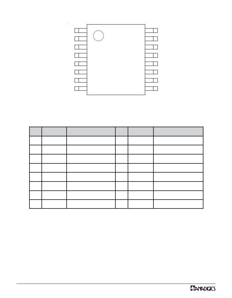
S7 Package
16 Pin Wide Body SOIC
with Heat Slug
RF Input
15dB
15dB
ACA1206
12dB
12dB
ACA0862B/D
RF Output
2
PRELIMINARY DATA SHEET - Rev 1.0
09/2005
ACA1206
Table 1: Pin Description
Figure 2: Pin Out
N
I
P
E
M
A
N
N
O
I
T
P
I
R
C
S
E
D
N
I
P
E
M
A
N
N
O
I
T
P
I
R
C
S
E
D
1
D
N
G
d
n
u
o
r
G
9
D
N
G
d
n
u
o
r
G
2
C
/
N
n
o
it
c
e
n
n
o
C
o
N
0
1
V
B
B
r
e
if
il
p
m
A
r
o
f
y
l
p
p
u
S
3
F
R
A
N
I
A
r
e
if
il
p
m
A
o
t
t
u
p
n
I
1
1
F
R
B
T
U
O
B
r
e
if
il
p
m
A
m
o
r
f
t
u
p
t
u
O
4
D
N
G
d
n
u
o
r
G
2
1
D
N
G
d
n
u
o
r
G
5
D
N
G
d
n
u
o
r
G
3
1
D
N
G
d
n
u
o
r
G
6
F
R
B
N
I
B
r
e
if
il
p
m
A
o
t
t
u
p
n
I
4
1
F
R
A
T
U
O
A
r
e
if
il
p
m
A
m
o
r
f
t
u
p
t
u
O
7
I
J
D
A
t
s
u
j
d
A
t
n
e
r
r
u
C
5
1
V
A
A
r
e
if
il
p
m
A
r
o
f
y
l
p
p
u
S
8
D
N
G
d
n
u
o
r
G
6
1
D
N
G
d
n
u
o
r
G
1
2
3
4
5
6
7
8
16
15
14
13
12
11
10
9
GND
GND
I
ADJ
RF
INA
GND
GND
GND
RF
OUTA
V
B
N/C
GND
RF
INB
GND
GND
RF
OUTB
V
A
PRELIMINARY DATA SHEET - Rev 1.0
09/2005
3
ACA1206
ELECTRICAL CHARACTERISTICS
Table 2: Absolute Minimum and Maximum Ratings
R
E
T
E
M
A
R
A
P
N
I
M
P
Y
T
X
A
M
T
I
N
U
y
c
n
e
u
q
e
r
F
F
R
0
4
-
0
0
0
1
z
H
M
V
:
y
l
p
p
u
S
D
D
)
5
1
,
4
1
,
1
1
,
0
1
s
n
i
p
(
-
2
1
+
-
C
D
V
e
r
u
t
a
r
e
p
m
e
T
g
n
it
a
r
e
p
O
0
4
-
-
0
1
1
+
O
C
Stresses in excess of the absolute ratings may cause permanent
damage. Functional operation is not implied under these conditions.
Exposure to absolute ratings for extended periods of time may
adversely affect reliability.
The device may be operated safely over these conditions; however,
parametric performance is guaranteed only over the conditions defined in
the electrical specifications.
R
E
T
E
M
A
R
A
P
N
I
M
X
A
M
T
I
N
U
)
5
1
,
4
1
,
1
1
,
0
1
s
n
i
p
(
s
e
il
p
p
u
S
r
e
if
il
p
m
A
0
5
1
+
C
D
V
)
6
,
3
s
n
i
p
(
r
e
w
o
P
t
u
p
n
I
F
R
-
0
7
+
V
m
B
d
e
r
u
t
a
r
e
p
m
e
T
e
g
a
r
o
t
S
5
6
-
0
5
1
+
C
∞
e
r
u
t
a
r
e
p
m
e
T
g
n
ir
e
d
l
o
S
-
0
6
2
+
C
∞
e
m
i
T
g
n
ir
e
d
l
o
S
-
0
.
5
c
e
s
Notes:
1. Pins 3 and 6 should be AC-coupled. No external DC bias should be
applied.
2. Pin 7 should be pulled to ground through resistor R1, as shown in Figure 3.
No external DC bias should be applied.
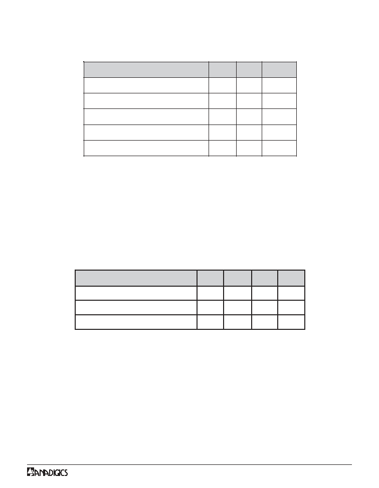
Table 3: Operating Ranges

4
PRELIMINARY DATA SHEET - Rev 1.0
09/2005
ACA1206
Table 4: Electrical Specifications
(T
A
= +25∞C, V
DD
= +12 VDC)
Notes:
(1) Measured with a balun on the input and output of the device. See Figure 3 for test setup.
(2) 15.6 dB tilt, 49 dBmV output (per channel) at 1002 MHz plus QAM set 6 dBmV down from carrier.
(3) 3 dB tilt, 37 dBmV output (per channel) at 1002 MHz plus QAM set 6 dBmV down from carrier.
(4) Tested with R1 = 5.265 k
V
(5) Tested with R1 = 1.866 k
V
R
E
T
E
M
A
R
A
P
N
I
M
P
Y
T
X
A
M
T
I
N
U
S
T
N
E
M
M
O
C
z
H
G
1
t
a
n
i
a
G
)
1
(
7
.
3
1
2
.
4
1
7
.
4
1
B
d
s
s
e
n
t
a
l
F
n
i
a
G
-
-
-
1
.
0
6 1
.
0
6 3
.
0
1
.
0
6 1
.
0
-
-
-
B
d
z
H
M
0
0
1
o
t
5
4
z
H
M
0
0
8
o
t
0
0
1
z
H
M
2
0
0
1
o
t
0
0
8
z
H
G
1
t
a
e
r
u
g
i
F
e
s
i
o
N
)
1
(
-
0
.
3
5
.
3
B
d
A
m
5
9
1
B
T
C
)
4
(
,
)
3
(
,
)
1
(
-
-
-
2
7
-
5
7
-
-
9
6
-
-
-
c
B
d
s
l
e
n
n
a
h
C
7
7
s
l
e
n
n
a
h
C
0
1
1
s
l
e
n
n
a
h
C
8
2
1
A
m
5
2
3
B
T
C
)
5
(
,
)
2
(
,
)
1
(
-
-
-
5
7
-
4
7
-
-
2
7
-
-
-
c
B
d
s
l
e
n
n
a
h
C
7
7
s
l
e
n
n
a
h
C
0
1
1
s
l
e
n
n
a
h
C
8
2
1
A
m
5
9
1
O
S
C
)
4
(
,
)
3
(
,
)
1
(
-
-
-
5
7
-
7
7
-
-
8
6
-
-
-
c
B
d
s
l
e
n
n
a
h
C
7
7
s
l
e
n
n
a
h
C
0
1
1
s
l
e
n
n
a
h
C
8
2
1
A
m
5
2
3
O
S
C
)
5
(
,
)
2
(
,
)
1
(
-
-
-
5
7
-
2
7
-
-
4
6
-
-
-
c
B
d
s
l
e
n
n
a
h
C
7
7
s
l
e
n
n
a
h
C
0
1
1
s
l
e
n
n
a
h
C
8
2
1
A
m
5
9
1
D
O
M
X
)
4
(
,
)
3
(
,
)
1
(
-
-
-
4
6
-
8
6
-
-
1
6
-
-
-
c
B
d
s
l
e
n
n
a
h
C
7
7
s
l
e
n
n
a
h
C
0
1
1
s
l
e
n
n
a
h
C
8
2
1
A
m
5
2
3
D
O
M
X
)
5
(
,
)
2
(
,
)
1
(
-
-
-
9
6
-
0
7
-
-
7
6
-
-
-
c
B
d
s
l
e
n
n
a
h
C
7
7
s
l
e
n
n
a
h
C
0
1
1
s
l
e
n
n
a
h
C
8
2
1
I
(
t
n
e
r
r
u
C
y
l
p
p
u
S
D
D
)
5
8
1
0
0
3
5
9
1
5
2
3
5
0
2
0
5
3
A
m
k
6
6
8
.
1
=
1
R
V
k
5
6
2
.
5
=
1
R
V
e
p
o
l
S
t
n
e
l
a
v
i
u
q
E
e
l
b
a
C
)
1
(
-
D
B
T
-
B
d
s
s
o
L
n
r
u
t
e
R
)
1
(
8
1
2
2
-
B
d
e
c
n
a
t
s
i
s
e
R
l
a
m
r
e
h
T
-
-
0
.
6
W
/
C
∞

PRELIMINARY DATA SHEET - Rev 1.0
09/2005
5
ACA1206
Figure 3: Test Circuit
1
2
3
4
5
6
7
8
9
10
11
12
13
14
15
16
ACA1206
15dB
15dB
N/C
.01 uF
+12 Vdc
390 nH
RF
IN
390 nH
RF Out
300pF
300pF
+12 Vdc
.01 uF
.01 uF
.01
uF
R1
See Table 5
Note: Apply voltage to both +12Vdc lines simultaneoulsy
T
N
E
R
R
U
C
L
A
N
I
M
O
N
1
R
A
m
5
9
1
k
6
6
8
.
1
V
A
m
5
2
3
k
5
6
2
.
5
V
Table 5
6
PRELIMINARY DATA SHEET - Rev 1.0
09/2005
ACA1206
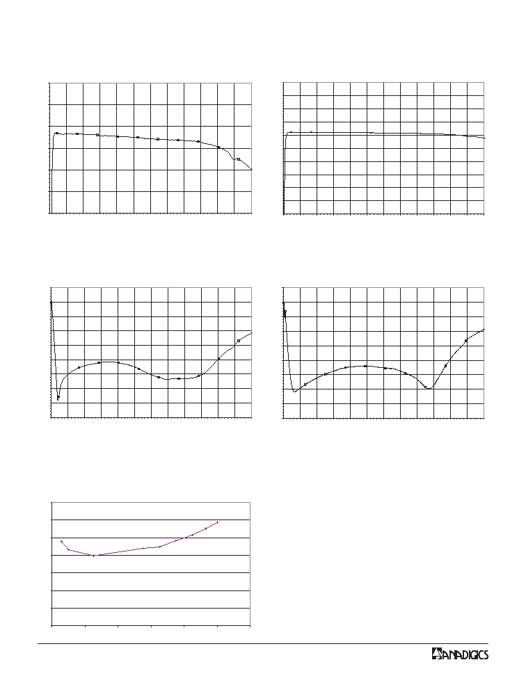
Figure 4: Gain vs. Frequency
(V
DD
= +12 V, I
DD
= 195 mA)
PERFORMANCE DATA
11
12
13
14
15
16
17
0
100
200
300
400
500
600
700
800
900
1000
1100
1200
Frequency (MHz)
S21 (
d
B)
-50
-45
-40
-35
-30
-25
-20
-15
-10
-5
0
0
100
200
300
400
500
600
700
800
900
1000
1100
1200
Frequency (MHz)
S12 (
d
B)
-40
-35
-30
-25
-20
-15
-10
-5
0
5
0
100
200
300
400
500
600
700
800
900
1000
1100
1200
Frequency (MHz)
S11 (
d
B)
-40
-35
-30
-25
-20
-15
-10
-5
0
5
0
100
200
300
400
500
600
700
800
900
1000
1100
1200
Frequency (MHz)
S22 (
d
B)
0
0.5
1
1.5
2
2.5
3
3.5
0
200
400
600
800
1000
1200
Frequency (MHz)
Noi
s
e Fi
gur
e
Figure 5: Reverse Isolation vs. Frequency
(V
DD
= +12 V, I
DD
= 195 mA)
Figure 6: Input Return Loss vs. Frequency
(V
DD
= +12 V, I
DD
= 195 mA)
Figure 7: Output Return Loss vs. Frequency
(V
DD
= +12 V, I
DD
= 195 mA)
Figure 8: Noise Figure vs. Frequency
(V
DD
= +12 V, I
DD
= 195 mA)

PRELIMINARY DATA SHEET - Rev 1.0
09/2005
7
ACA1206
-90
-85
-80
-75
-70
-65
-60
0
100
200
300
400
500
600
Frequency (MHz)
CTB (dBc
)
-95
-90
-85
-80
-75
-70
-65
-60
0
100
200
300
400
500
600
Frequency (MHz)
CSO (dBc)
-80
-78
-76
-74
-72
-70
-68
-66
-64
-62
-60
0
100
200
300
400
500
600
Frequency (MHz)
XMO
D
(
d
Bc)
Figure 9: CTB vs. Frequency
(V
DD
= +12 V, I
DD
= 195 mA, 79 Analog Channels, 3 dB Tilt, +37 dBmV output power at 1 GHz)
Figure 10: CSO vs. Frequency
(V
DD
= +12 V, I
DD
= 195 mA, 79 Analog Channels, 3 dB Tilt, +37 dBmV output power at 1 GHz)
Figure 11: XMOD vs. Frequency
(V
DD
= +12 V, I
DD
= 195 mA, 79 Analog Channels, 3 dB Tilt, +37 dBmV output power at 1 GHz)

8
PRELIMINARY DATA SHEET - Rev 1.0
09/2005
ACA1206
-90
-85
-80
-75
-70
-65
-60
0
100
200
300
400
500
600
700
800
Frequency (MHz)
CTB (dBc)
-100
-95
-90
-85
-80
-75
-70
-65
-60
0
100
200
300
400
500
600
700
800
Frequency (MHz)
CSO (dBc)
-80
-78
-76
-74
-72
-70
-68
-66
-64
-62
-60
0
100
200
300
400
500
600
700
800
Frequency (MHz)
XMO
D
(
d
Bc)
Figure 12: CTB vs. Frequency
(V
DD
= +12 V, I
DD
= 195 mA, 112 Analog Channels, 3 dB Tilt, +37 dBmV output power at 1 GHz)
Figure 13: CSO vs. Frequency
(V
DD
= +12 V, I
DD
= 195 mA, 112 Analog Channels, 3 dB Tilt, +37 dBmV output power at 1 GHz)
Figure 14: XMOD vs. Frequency
(V
DD
= +12 V, I
DD
= 195 mA, 112 Analog Channels, 3 dB Tilt, +37 dBmV output power at 1 GHz)
PRELIMINARY DATA SHEET - Rev 1.0
09/2005
9
ACA1206
12
12.5
13
13.5
14
14.5
15
15.5
16
16.5
17
0
100
200
300
400
500
600
700
800
900
1000
1100
1200
Frequency (MHz)
S21 (
d
B)
-50
-45
-40
-35
-30
-25
-20
-15
-10
-5
0
0
100
200
300
400
500
600
700
800
900
1000
1100
1200
Frequency (MHz)
S12 (
d
B)
-40
-35
-30
-25
-20
-15
-10
-5
0
5
0
100
200
300
400
500
600
700
800
900
1000
1100
1200
Frequency (MHz)
S11 (
d
B)
-40
-35
-30
-25
-20
-15
-10
-5
0
5
0
100
200
300
400
500
600
700
800
900
1000
1100
1200
Frequency (MHz)
S22 (
d
B)
0
0.5
1
1.5
2
2.5
3
3.5
0
200
400
600
800
1000
1200
Frequency(MHz)
No
ise F
i
g
u
re
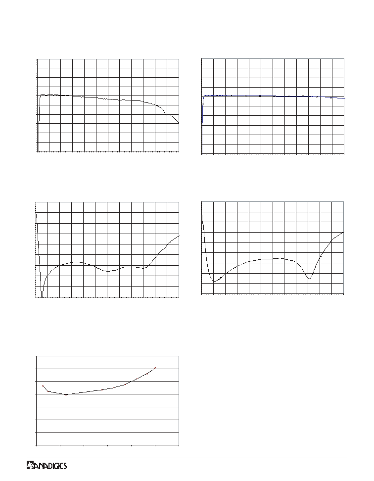
Figure 15: Gain vs. Frequency
(V
DD
= +12 V, I
DD
= 325 mA)
Figure 16: Reverse Isolation vs. Frequency
(V
DD
= +12 V, I
DD
= 325 mA)
Figure 17: Input Return Loss vs. Frequency
(V
DD
= +12 V, I
DD
= 325 mA)
Figure 18: Output Return Loss vs. Frequency
(V
DD
= +12 V, I
DD
= 325 mA)
Figure 19: Noise Figure vs. Frequency
(V
DD
= +12 V, I
DD
= 325 mA)

10
PRELIMINARY DATA SHEET - Rev 1.0
09/2005
ACA1206
-90
-85
-80
-75
-70
-65
-60
0
100
200
300
400
500
600
Frequency (MHz)
CTB (dBc
)
-100
-95
-90
-85
-80
-75
-70
-65
-60
0
100
200
300
400
500
600
Frequency (MHz)
CS
O (dBc)
-80
-78
-76
-74
-72
-70
-68
-66
-64
-62
-60
0
100
200
300
400
500
600
Frequency (MHz)
XMO
D
(
d
Bc)
Figure 20: CTB vs. Frequency
(V
DD
= +12 V, I
DD
= 325 mA, 79 Analog Channels, 15.6 dB Tilt, +49 dBmV output power at 1 GHz)
Figure 21: CSO vs. Frequency
(V
DD
= +12 V, I
DD
= 325 mA, 79 Analog Channels, 15.6 dB Tilt, +49 dBmV output power at 1 GHz)
Figure 22: XMOD vs. Frequency
(V
DD
= +12 V, I
DD
= 325 mA, 79 Analog Channels, 15.6 dB Tilt, +49 dBmV output power at 1 GHz)

PRELIMINARY DATA SHEET - Rev 1.0
09/2005
11
ACA1206
-90
-85
-80
-75
-70
-65
-60
0
100
200
300
400
500
600
700
800
Frequency (MHz)
CTB (dBc)
-100
-95
-90
-85
-80
-75
-70
-65
-60
0
100
200
300
400
500
600
700
800
Frequency (MHz)
CSO (dBc)
-80
-78
-76
-74
-72
-70
-68
-66
-64
-62
-60
0
100
200
300
400
500
600
700
800
Frequency (MHz)
XMO
D
(
d
Bc)
Figure 23: CTB vs. Frequency
(V
DD
= +12 V, I
DD
= 325 mA, 112 Analog Channels, 15.6 dB Tilt, +49 dBmV output power at 1 GHz)
Figure 24: CSO vs. Frequency
(V
DD
= +12 V, I
DD
= 325 mA, 112 Analog Channels, 15.6 dB Tilt, +49 dBmV output power at 1 GHz)
Figure 25: XMOD vs. Frequency
(V
DD
= +12 V, I
DD
= 325 mA, 112 Analog Channels, 15.6 dB Tilt, +49 dBmV output power at 1 GHz)

12
PRELIMINARY DATA SHEET - Rev 1.0
09/2005
ACA1206
Figure 27: Evaluation Board Schematic
APPLICATION INFORMATION
The ACA1206 is designed as an input stage. This
part can be used alone for low gain, low output level
applications or can be cascaded with one of the
ACA0862 output stages for higher gain and output
signal drive level. The ACA1206 is a low power
dissipation part designed as a driver for the
ACA0862B output stage.
Figure 26: Evaluation Board Layout
Title
1
2
3
4
5
6
7
8
9
10
11
12
13
14
15
16
NC
C1
C2
C3
C4
C5
C6
T1
RF OUT
RF IN
R1
L1
L2
+1
2
V
T2
+1
2
V
TVS
+
C7
ACA1206
C9

PRELIMINARY DATA SHEET - Rev 1.0
09/2005
13
ACA1206
Table 6: Evaluation Board Parts List
Notes:
1. T1, T2 (balun) wind 4 turns thru core as shown. (Figure 28).
2. "N" connector,center pin,should be approximately 80 mils in length.
3. Due to the high power dissapation of this devide the PC board should be mounted/ attached to a large heat
sink.
(4) See Table 5.
Figure 28: Balun Drawing
M
E
T
I
N
O
I
T
P
I
R
C
S
E
D
Y
T
Q
R
O
D
N
E
V
N
/
P
R
O
D
N
E
V
6
C
,
5
C
,
2
C
,
1
C
.
P
A
C
P
I
H
C
.
F
u
1
0
.
0
4
A
T
A
R
U
M
V
5
2
K
3
0
1
1
R
7
X
9
3
M
R
G
4
C
,
3
C
.
P
A
C
P
I
H
C
.
F
p
0
7
4
2
A
T
A
R
U
M
V
5
2
K
1
0
3
R
7
X
7
4
M
R
G
7
C
.
P
A
C
.
T
C
E
L
E
F
u
7
4
1
.
P
R
O
C
Y
E
K
-I
G
I
D
D
N
-
5
7
2
5
P
9
C
D
E
S
U
T
O
N
2
L
,
1
L
.
D
N
I
P
I
H
C
H
n
0
7
4
2
A
T
A
R
U
M
2
5
0
4
/
3
0
-
O
O
N
O
K
7
4
R
N
1
H
Q
L
N
U
L
A
B
-
2
T
,
1
T
E
R
O
C
2
e
ti
R
-
r
i
a
F
2
0
7
2
0
0
3
4
8
2
E
R
I
W
.
d
n
I
e
r
i
W
S
W
M
0
2
-
9
2
4
1
6
3
2
-
T
1
R
)
4
(
k
7
8
.
1
V
7
2
.
5
k
V
1
c
i
n
o
s
a
n
a
P
V
1
7
8
1
F
K
E
3
-
J
R
E
V
1
3
2
5
F
K
E
3
-
J
R
E
S
V
T
T
T
A
W
0
0
6
.
T
L
O
V
2
1
S
V
T
1
.
P
R
O
C
Y
E
K
-I
G
I
D
D
N
-
T
C
C
C
A
2
1
J
B
M
S
R
O
T
C
E
N
N
O
C
5
7
V
.
T
N
U
O
M
L
E
N
A
P
E
L
A
M
N
2
K
C
A
N
R
E
T
S
A
P
.
P
R
E
T
N
E
4
0
5
4
E
P
D
R
A
O
B
T
I
U
C
R
I
C
D
E
T
N
I
R
P
1
M
U
I
D
N
I
S
L
I
M
0
6
1
x
0
0
3
1
.
P
R
O
C
M
U
I
D
N
I
A
C
I
R
E
M
A
F
O
Y
6
9
9
4
1

14
PRELIMINARY DATA SHEET - Rev 1.0
09/2005
ACA1206
PACKAGE OUTLINE
Figure 29: S7 Package Outline - 16 Pin Wide Body SOIC with Heat Slug

PRELIMINARY DATA SHEET - Rev 1.0
09/2005
15
ACA1206
NOTES

WARNING
ANADIGICS products are not intended for use in life support appliances, devices or systems. Use of an ANADIGICS
product in any such application without written consent is prohibited.
IMPORTANT NOTICE
ANADIGICS, Inc.
141 Mount Bethel Road
Warren, New Jersey 07059, U.S.A.
Tel: +1 (908) 668-5000
Fax: +1 (908) 668-5132
URL: http://www.anadigics.com
E-mail: Mktg@anadigics.com
ANADIGICS, Inc. reserves the right to make changes to its products or to discontinue any product at any time without
notice. The product specifications contained in Advanced Product Information sheets and Preliminary Data Sheets are
subject to change prior to a product's formal introduction. Information in Data Sheets have been carefully checked and are
assumed to be reliable; however, ANADIGICS assumes no responsibilities for inaccuracies. ANADIGICS strongly urges
customers to verify that the information they are using is current before placing orders.
PRELIMINARY DATA SHEET - Rev 1.0
09/2005
16
ACA1206
ORDERING INFORMATION
R
E
B
M
U
N
R
E
D
R
O
E
R
U
T
A
R
E
P
M
E
T
E
G
N
A
R
E
G
A
K
C
A
P
N
O
I
T
P
I
R
C
S
E
D
G
N
I
G
A
K
C
A
P
T
N
E
N
O
P
M
O
C
2
P
7
S
R
6
0
2
1
A
C
A
C
∞
0
1
1
o
t
C
∞
0
4
-
t
n
a
il
p
m
o
C
-
S
H
o
R
y
d
o
B
e
d
i
W
n
i
P
6
1
k
n
i
S
t
a
e
H
h
ti
w
C
I
O
S
l
e
e
R
&
e
p
a
T
e
c
e
i
P
0
0
5
,
1