Microsoft Word - LP62S16256F-T.doc
LP62S16256F-T Series
256K X 16 BIT LOW VOLTAGE CMOS SRAM
(August, 2005, Version 1.0)
AMIC Technology, Corp.
Document Title
256K X 16 BIT LOW VOLTAGE CMOS SRAM
Revision History
Rev. No. History Issue
Date Remark
0.3
Change operation voltage from 2.7V~3.3V to 2.7V~3.6V
November 22, 2002
Preliminary
Add 55ns specification
0.4 Change
I
CC2
from 15mA to 8mA
April 18, 2003
0.5
Modify 48LD CSP bottom view outline drawing
May 5, 2003
0.6
Modify 48LD CSP outline dimensions
November 19, 2003
0.7
Add Pb-Free package type
August 9, 2004
1.0
Final version release
August 23, 2005
Final
LP62S16256F-T Series
256K X 16 BIT LOW VOLTAGE CMOS SRAM
(August, 2005, Version 1.0)
1
AMIC Technology, Corp.
Features
Operating voltage: 2.7V to 3.6V
Access times: 55ns / 70ns (max.)
Current:
Very low power version: Operating: 40mA (max.)
Standby: 10
µ
A (max.)
Full static operation, no clock or refreshing required
All inputs and outputs are directly TTL-compatible
Common I/O using three-state output
Data retention voltage: 2.0V (min.)
Available in 44-pin TSOP and 48-ball CSP (6
×
8mm)
packages
General Description
The LP62S16256F-T is a low operating current 4,194,304-bit
static random access memory organized as 262,144 words
by 16 bits and operates on low power voltage from 2.7V to
3.6V. It is built using AMIC's high performance CMOS
process.
Inputs and three-state outputs are TTL compatible and allow
for direct interfacing with common system bus structures.
The chip enable input is provided for POWER-DOWN, device
enable. Two byte enable inputs and an output enable input
are included for easy interfacing.
Data retention is guaranteed at a power supply voltage as low
as 2.0V.
Product Family
Power Dissipation
Product Family
Operating
Temperature
VCC
Range
Speed
Data Retention
(I
CCDR
, Typ.)
Standby
(I
SB1
, Typ.)
Operating
(I
CC2
, Typ.)
Package
Type
LP62S16256F-T
-25
°
C ~ +85
°
C
2.7V~3.6V
55ns / 70ns
0.08
µ
A 0.3
µ
A
5mA
44L TSOP
48B CSP
1. Typical values are measured at VCC = 3.0V, T
A
= 25
°
C and not 100% tested.
2. Data retention current VCC = 2.0V.
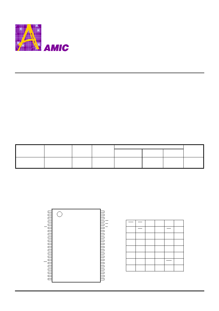
Pin Configurations
TSOP
CSP (Chip Size Package)
48-pin Top View
I/O
9
I/O
10
GND
VCC
I/O
15
I/O
16
NC
A8
NC
A9
A12
A10
A11
NC
A13
A14
A15
I/O
8
I/O
7
I/O
3
I/O
1
GND
VCC
A0
A3
A5
A6
A4
A1
A2
NC
6
5
4
3
2
1
A
B
C
D
E
F
G
H
I/O
14
I/O
13
I/O
12
I/O
11
A17
NC
A7
A16
I/O
2
I/O
4
I/O
5
I/O
6
LB
HB
WE
OE
CE
1
2
3
4
5
6
7
8
9
10
11
12
13
14
15
16
17
18
19
20
21
22
A3
A2
A1
A0
CE
I/O
1
I/O
2
I/O
3
I/O
4
VCC
GND
I/O
5
I/O
6
I/O
7
I/O
8
WE
A17
A16
A15
A14
44
43
42
41
40
39
38
37
36
35
34
33
32
31
30
29
28
27
26
25
24
23
A11
A10
A9
A8
NC
I/O
9
I/O
10
I/O
11
I/O
12
VCC
GND
I/O
13
I/O
14
I/O
15
I/O
16
LB
HB
OE
A7
A6
LP62S16256FV-T
A13
A5
A4
A12
LP62S16256F-T Series
(August, 2005, Version 1.0)
2
AMIC Technology, Corp.
Block Diagram
DECODER
512 X 8192
MEMORY ARRAY
COLUMN I/O
INPUT
DATA
CIRCUIT
CONTROL
CIRCUIT
VCC
GND
I/O
8
I/O
1
A17
A16
A0
WE
HB
INPUT
DATA
CIRCUIT
I/O
9
I/O
16
LB
OE
CE
Pin Descriptions -- TSOP
Pin No.
Symbol
Description
1 - 5, 18 - 27,
42 - 44
A0 - A17
Address Inputs
6
CE
Chip Enable Input
7 - 10, 13 - 16,
29 - 32, 35 - 38
I/O
1
- I/O
16
Data
Inputs/Outputs
17
WE
Write Enable Input
39
LB
Lower Byte Enable Input (I/O
1
to I/O
8
)
40
HB
Higher Byte Enable Input (I/O
9
to I/O
16
)
41
OE
Output Enable Input
11, 33
VCC
Power
12, 34
GND
Ground
28 NC
No
Connection
LP62S16256F-T Series
(August, 2005, Version 1.0)
3
AMIC Technology, Corp.
Pin Description - CSP
Symbol Description Symbol Description
A0 - A17
Address Inputs
HB
Higher Byte Enable Input
(I/O
9
- I/O
16
)
CE
Chip Enable
OE
Output Enable
I/O
1
- I/O
16
Data Input/Output
VCC
Power Supply
WE
Write Enable Input
GND
Ground
LB
Byte Enable Input
(I/O
1
- I/O
8
)
NC No
Connection
Recommended DC Operating Conditions
(T
A
= -25
°
C to + 85
°
C)
Symbol Parameter Min.
Typ.
Max. Unit
VCC Supply
Voltage
2.7
3
3.6
V
GND
Ground
0 0 0
V
V
IH
Input High Voltage
2.2
-
VCC + 0.3
V
V
IL
Input Low Voltage
-0.3
-
+0.6
V
C
L
Output
Load
-
-
30
pF
TTL Output
Load
-
-
1
-
LP62S16256F-T Series
(August, 2005, Version 1.0)
4
AMIC Technology, Corp.
Absolute Maximum Ratings*
VCC to GND .............................................. -0.5V to +4.0V
IN, IN/OUT Volt to GND................... -0.5V to VCC + 0.5V
Operating Temperature, Topr ...................-25
°
C to +85
°
C
Storage Temperature, Tstg.....................-55
°
C to +125
°
C
Power Dissipation, P
T.......................................................................
0.7W
*Comments
Stresses above those listed under "Absolute Maximum
Ratings" may cause permanent damage to this device.
These are stress ratings only. Functional operation of this
device at these or any other conditions above those
indicated in the operational sections of this specification is
not implied or intended. Exposure to the absolute
maximum rating conditions for extended periods may affect
device reliability.
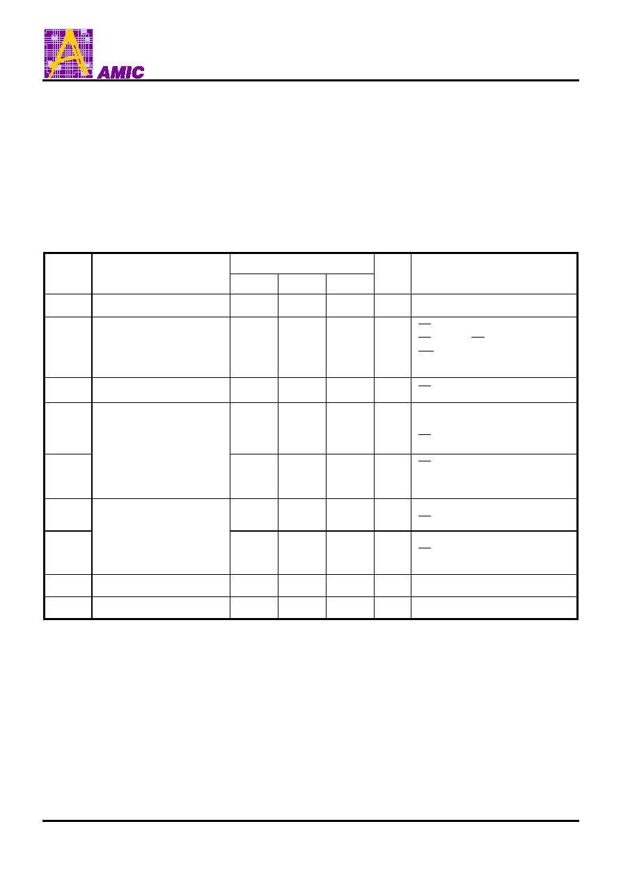
DC Electrical Characteristics
(T
A
= -25
°
C to + 85
°
C, VCC = 2.7V to 3.6V, GND = 0V)
Symbol Parameter LP62S16256F-55LLT / 70LLT
Unit
Conditions
Min.
Typ.
Max.
I
LI
Input Leakage Current
-
-
1
µ
A
V
IN
= GND to VCC
I
LO
Output Leakage Current
-
-
1
µ
A
CE = V
IH
HB = V
IH
or OE = V
IH
or
WE = V
IH
V
I/O
= GND to VCC
I
CC
Active Power Supply Current
-
-
5
mA
CE = V
IL
, I
I/O
= 0mA
I
CC1
-
25
40
mA
Min. Cycle, Duty = 100%
Dynamic
Operating
CE = V
I
, I
I/O
= 0mA
I
CC2
Current
- 5 8
mA
CE = V
IL
, V
IH
= VCC,
V
IL
= 0V, f = 1MHz,
I
I/O
= 0 mA
I
SB
-
-
1 mA
VCC
3.3V
CE = V
IH
I
SB1
Standby Current
- 0.3 10
µ
A
VCC
3.3V
CE
VCC - 0.2V,
V
IN
0V
V
OL
Output Low Voltage
-
-
0.4
V
I
OL
= 2.1 mA
V
OH
Output High Voltage
2.2
-
-
V
I
OH
= -1.0 mA