Microsoft Word - A48P3616 naya.doc
A48P3616
Preliminary
8M X 16 Bit DDR DRAM
Preliminary (September 2005, Version 0.0)
AMIC Technology, Corp.
Document Title
8M X 16 Bit DDR DRAM
Revision History
Rev. No. History Issue
Date Remark
0.0 Initial
issue
September 5, 2005
Preliminary
A48P3616
Preliminary
8M X 16 Bit DDR DRAM
Preliminary (September 2005, Version 0.0)
1
AMIC Technology, Corp.
Feature
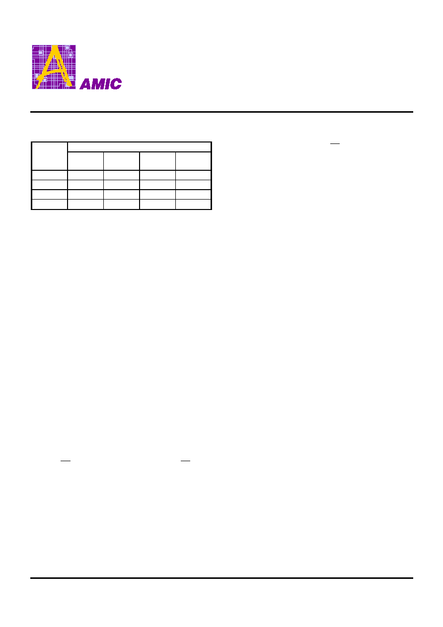
CAS Latency and Frequency
Maximum Operating Frequency (MHz)
CAS
Latency
DDR466
(43)
DDR400
(5T)
DDR333
(6K)
DDR266
(75B)
2 - - 133
100
2.5 - 166 166 133
3 233 200 - -
· Double data rate architecture: two data transfers per clock
cycle.
· Bidirectional data strobe (DQS) is transmitted and received
with data, to be used in capturing data at the receiver.
· DQS is edge-aligned with data for reads and is center-
aligned with data for writes.
· Differential clock inputs (CK and CK )
· Four internal banks for concurrent operation
· Data mask (DM) for write data.
· DLL aligns DQ and DQS transitions with CK transitions.
· Commands entered on each positive CK edge; data and
data mask referenced to both edges of DQS.
· Burst lengths: 2, 4, or 8
· CAS Latency: 2 & 2.5 for 6K/75B, 2.5 & 3 for 5T, 3 for 43
· Auto Precharge option for each burst access
· Auto Refresh and Self Refresh Modes
· 15.6µs Maximum Average Periodic Refresh Interval
· 2.5V (SSTL_2 compatible) I/O
· V
DD
= V
DDQ
= 2.5V
±
0.2V (6K/75B)
· V
DD
= V
DDQ
= 2.6V
±
0.1V (5T/43)
· Lead-free and Halogen-free product available
General Description
The 128Mb DDR SDRAM is a high-speed CMOS, dynamic
random-access memory containing 134,217,728 bits. It is
internally configured as a quad-bank DRAM and is based on
Nanya's 110nm process.
The 128Mb DDR SDRAM uses a double-data-rate
architecture to achieve high-speed operation. The double
data rate architecture is essentially a 2n prefetch architecture
with an interface designed to transfer two data words per
clock cycle at the I/O pins. A single read or write access for
the 128Mb DDR SDRAM effectively consists of a single 2n-bit
wide, one clock cycle data transfer at the internal DRAM core
and two corresponding n-bit wide, one-half-clock-cycle data
transfers at the I/O pins.
A bidirectional data strobe (DQS) is transmitted externally,
along with data, for use in data capture at the receiver. DQS
is a strobe transmitted by the DDR SDRAM during Reads and
by the memory controller during Writes. DQS is edgealigned
with data for Reads and center-aligned with data for Writes.
The 128Mb DDR SDRAM operates from a differential clock
(CK and CK ; the crossing of CK going high and CK going
LOW is referred to as the positive edge of CK). Commands
(address and control signals) are registered at every positive
edge of CK. Input data is registered on both edges of DQS,
and output data is referenced to both edges of DQS, as well
as to both edges of CK.
Read and write accesses to the DDR SDRAM are burst
oriented; accesses start at a selected location and continue
for a programmed number of locations in a programmed
sequence.
Accesses begin with the registration of an Active command,
which is then followed by a Read or Write command. The
address bits registered coincident with the Active command
are used to select the bank and row to be accessed. The
address bits registered coincident with the Read or Write
command are used to select the bank and the starting column
location for the burst access.
The DDR SDRAM provides for programmable Read or Write
burst lengths of 2, 4, or 8 locations. An Auto Precharge
function may be enabled to provide a self-timed row
precharge that is initiated at the end of the burst access.
As with standard SDRAMs, the pipelined, multibank
architecture of DDR SDRAMs allows for concurrent operation,
thereby providing high effective bandwidth by hiding row
precharge and activation time.
An auto refresh mode is provided along with a power-saving
Power Down mode.
Prior to normal operation, the DDR SDRAM must be
initialized. The following sections provide detailed information
covering device initialization, register definition, command
descriptions and device operation.
The functionality described and the timing specifications
included in this data sheet are for the DLL Enabled mode of
operation.
A48P3616
Preliminary
8M X 16 Bit DDR DRAM
Preliminary (September 2005, Version 0.0)
2
AMIC Technology, Corp.
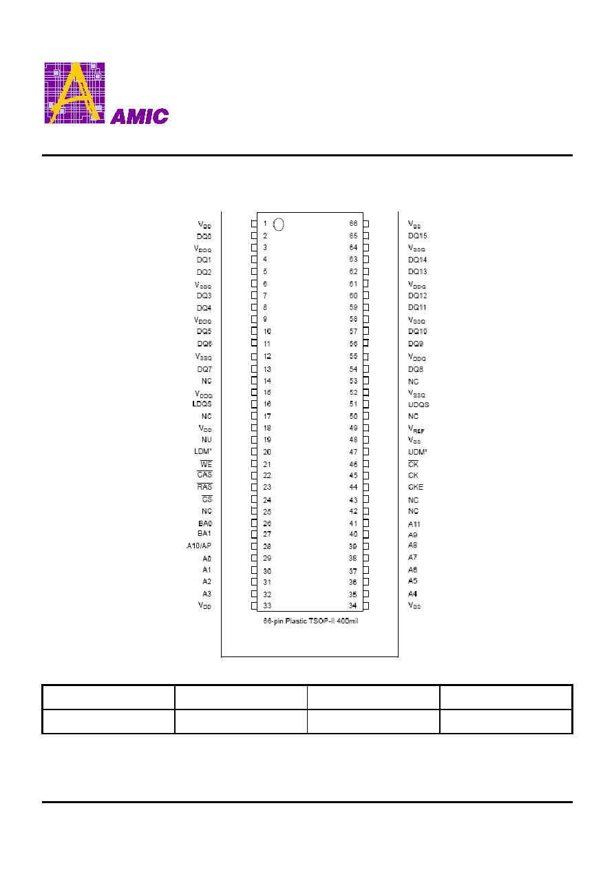
Pin Configuration
TSOP (II)
Column Address Table
Organization
Row Address
Column Address
Refresh
8Mb x 16
A0 A11
A0 A8
4K/64ms
A48P3616
Preliminary
8M X 16 Bit DDR DRAM
Preliminary (September 2005, Version 0.0)
3
AMIC Technology, Corp.
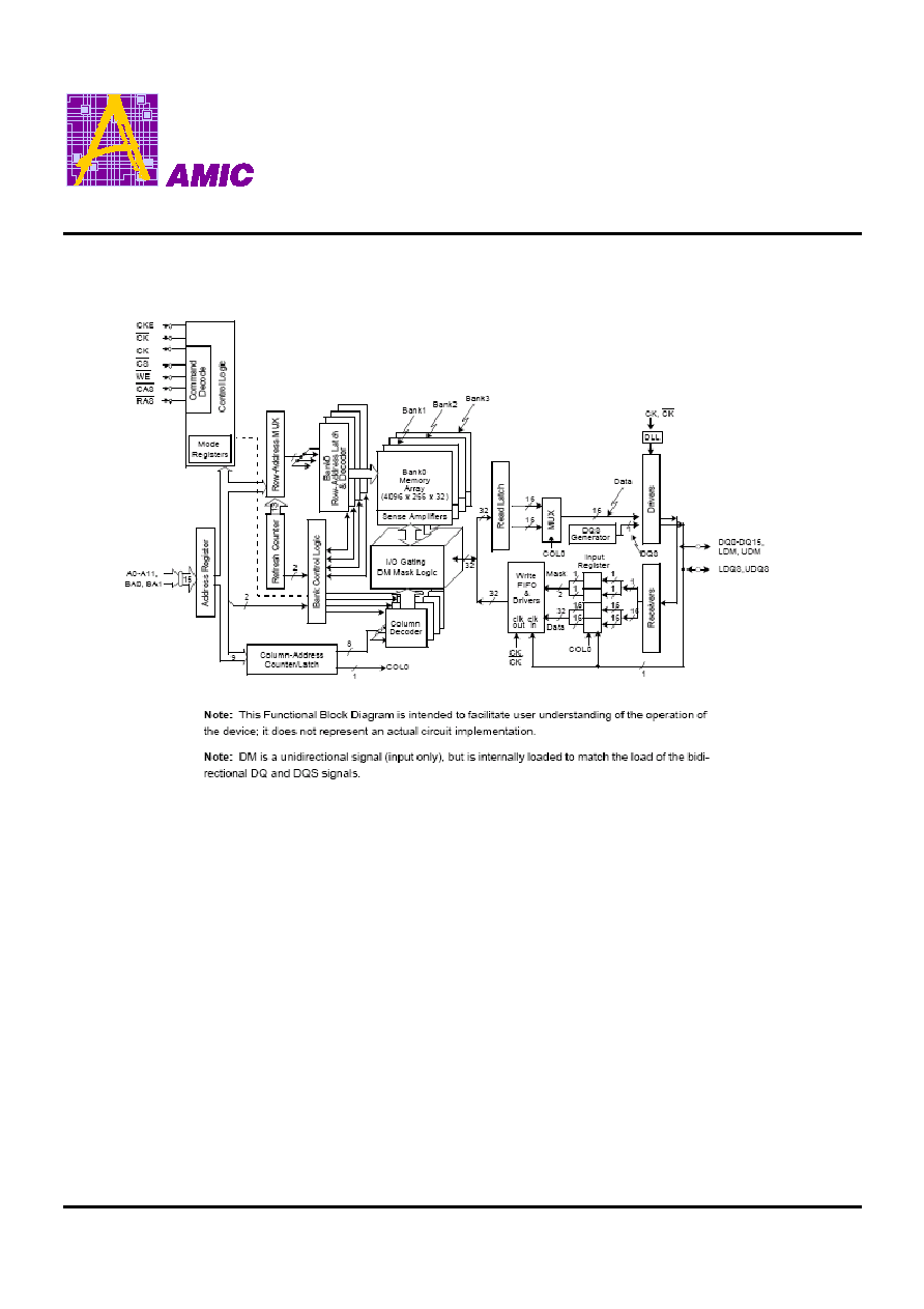
Block Diagram
A48P3616
Preliminary
8M X 16 Bit DDR DRAM
Preliminary (September 2005, Version 0.0)
4
AMIC Technology, Corp.
Input/Output Functional Description
Symbol
Type
Function
CK,
CK
Input
Clock: CK and
CK
are differential clock inputs. All address and control input signals are
sampled on the crossing of the positive edge of CK and negative edge of
CK
. Output
(read) data is referenced to the crossings of CK and
CK
(both directions of crossing).
CKE, CKE1, CKE1
Input
Clock Enable: CKE HIGH activates, and CKE Low deactivates, internal clock signals and
device input buffers and output drivers. Taking CKE Low provides Precharge Power Down
and Self Refresh operation (all banks idle), or Active Power Down (row Active in any bank).
CKE is synchronous for power down entry and exit, and for self refresh entry. CKE is
asynchronous for self refresh exit. CKE must be maintained high throughout read and write
accesses. Input buffers, excluding CK,
CK
and CKE are disabled during Power Down.
Input buffers, excluding CKE, are disabled during self refresh. The standard pinout includes
one CKE pin. Optional pinouts might include CKE1 on a different pin, in addition to CKE0,
to facilitate independent power down control of stacked devices.
CS
,
CS0
,
CS1
Input
Chip Select: All commands are masked when
CS
is registered high.
CS
provides for
external bank selection on systems with multiple banks.
CS
is considered part of the
command code. The standard pinout includes one
CS
pin. Optional pinouts might include
CS1
on a different pin, in addition to
CS0
, to allow upper or lower deck selection on
stacked devices.
RAS
,
CAS
,
WE
Input
Command Inputs:
RAS
,
CAS
and
WE
(along with
CS
) define the command being
entered.
DM Input
Input Data Mask: DM is an input mask signal for write data. Input data is masked when DM
is sampled high coincident with that input data during a Write access. DM is sampled on
both edges of DQS. Although DM pins are input only, the DM loading matches the DQ and
DQS loading. During a Read, DM can be driven high, low, or floated.
BA0, BA1
Input
Bank Address Inputs: BA0 and BA1 define to which bank an Active, Read, Write or
Precharge command is being applied. BA0 and BA1 also determines if the mode register or
extended mode register is to be accessed during a MRS or EMRS cycle.
A0 A11
Input
Address Inputs: Provide the row address for Active commands, and the column address
and Auto Precharge bit for Read/Write commands, to select one location out of the memory
array in the respective bank. A10 is sampled during a Precharge command to determine
whether the Precharge applies to one bank (A10 low) or all banks (A10 high). If only one
bank is to be precharged, the bank is selected by BA0, BA1. The address inputs also
provide the op-code during a Mode Register Set command.
DQ Input/Output Data Input/Output: Data bus.
DQS, LDQS, UDQS Input/Output
Data Strobe: Output with read data, input with write data. Edge-aligned with read data,
centered in write data. Used to capture write data. For the x16, LDQS corresponds to the
data on DQ0- DQ7; UDQS corresponds to the data on DQ8-DQ15
NC
No Connect: No internal electrical connection is present.
NU
Electrical connection is present. Should not be connected at second level of assembly.
VDDQ Supply
DQ Power Supply: 2.5V
±
0.2V.
VSSQ Supply
DQ Ground
VDD Supply
Power Supply: 2.5V
±
0.2V.
VSS Supply
Ground
VREF Supply
SSTL_2 reference voltage: (V
DDQ
/ 2)
±
1%.