
This document contains information on a product under development at FASL LLC. The information is intended to help you evaluate this product. FASL LLC reserves the
right to change or discontinue work on this proposed product without notice.
Publication Number 27024 Revision A Amendment 5 Issue Date June 18, 2004
PRELIMINARY
INFORMATION
Am29BDS128H/Am29BDS064H
128 or 64 Megabit (8 M or 4 M x 16-Bit)
CMOS 1.8 Volt-only Simultaneous Read/Write, Burst Mode
Flash Memory
Datasheet
Distinctive Characteristics
Architectural Advantages
Single 1.8 volt read, program and erase (1.65 to
1.95 volt)
Manufactured on 0.13 µm process technology
VersatileIOTM (V
IO
) Feature
-- Device generates data output voltages and tolerates
data input voltages as determined by the voltage on
the V
IO
pin
-- 1.8V compatible I/O signals
Simultaneous Read/Write operation
-- Data can be continuously read from one bank while
executing erase/program functions in other bank
-- Zero latency between read and write operations
-- Four bank architecture:
128 Mb has 16/48/48/16 Mbit banks
64 Mb has 8/24/24/8 Mbit banks
Programable Burst Interface
-- 2 Modes of Burst Read Operation
-- Linear Burst: 8, 16, and 32 words with wrap-around
-- Continuous Sequential Burst
SecSi
TM
(Secured Silicon) Sector region
-- Up to 128 words accessible through a command
sequence
-- Up to 64 factory-locked words
-- Up to 64 customer-lockable words
Sector Architecture
-- Banks A and D each contain both 4 Kword sectors
and 32 Kword sectors; Banks B and C contain ninety-
six 32 Kword sectors
-- Sixteen 4 Kword boot sectors
Half of the boot sectors are at the top of the address
range; half are at the bottom of address range
100,000 erase cycles per sector typical
20 year data retention typical
80-ball FBGA package (128 Mb) or 64-ball FBGA
(64 Mb) package
Performance Characteristics
Read access times at 75/66/54 MHz (C
L
=30 pF)
-- Burst access times of 9.3/11/13.5 ns at industrial
temperature range
-- Synchronous latency of 49/56/69 ns
-- Asynchronous random access times of 45/50/55 ns
Power dissipation (typical values, C
L
= 30 pF)
-- Burst Mode Read: 10 mA
-- Simultaneous Operation: 25 mA
-- Program/Erase: 15 mA
-- Standby mode: 0.2 µA
Hardware Features
Handshaking feature
-- Provides host system with minimum possible latency
by monitoring RDY
-- Reduced Wait-state handshaking option further
reduces initial access cycles required for burst
accesses beginning on even addresses
Hardware reset input (RESET#)
-- Hardware method to reset the device for reading
array data
WP# input
-- Write protect (WP#) function allows protection of the
four highest and four lowest 4 kWord boot sectors,
regardless of sector protect status
Persistent Sector Protection
-- A command sector protection method to lock
combinations of individual sectors and sector groups
to prevent program or erase operations within that
sector
-- Sectors can be locked and unlocked in-system at V
CC
level
Password Sector Protection
-- A sophisticated sector protection method to lock
combinations of individual sectors and sector groups
to prevent program or erase operations within that
sector using a user-defined 64-bit password
ACC input: Acceleration function reduces
programming time; all sectors locked when ACC =
V
IL
CMOS compatible inputs, CMOS compatible outputs
Low V
CC
write inhibit
Software Features
Supports Common Flash Memory Interface (CFI)
Software command set compatible with JEDEC
42.4 standards
-- Backwards compatible with Am29F and Am29LV
families
June 18, 2004 27024_A5_00_E
Am29BDS128H/Am29BDS064H
3
P r e l i m i n a r y I n f o r m a t i o n
General Description
The Am29BDS128H/Am29BDS064H is a 128 or 64 Mbit, 1.8 Volt-only, simulta-
neous Read/Write, Burst Mode Flash memory device, organized as 8,388,608 or
4,194,304 words of 16 bits each. This device uses a single V
CC
of 1.65 to 1.95 V
to read, program, and erase the memory array. A 12.0-volt V
HH
on ACC may be
used for faster program performance if desired. The device can also be pro-
grammed in standard EPROM programmers.
At 75 MHz, the device provides a burst access of 9.3 ns at 30 pF with a latency
of 49 ns at 30 pF. At 66 MHz, the device provides a burst access of 11 ns at 30
pF with a latency of 56 ns at 30 pF. At 54 MHz, the device provides a burst access
of 13.5 ns at 30 pF with a latency of 69ns at 30 pF. The device operates within
the industrial temperature range of -40°C to +85°C. The device is offered in
FBGA packages.
The Simultaneous Read/Write architecture provides simultaneous operation
by dividing the memory space into four banks. The device can improve overall
system performance by allowing a host system to program or erase in one bank,
then immediately and simultaneously read from another bank, with zero latency.
This releases the system from waiting for the completion of program or erase op-
erations.
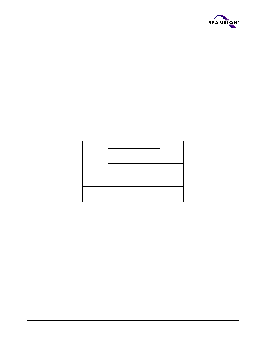
The device is divided as shown in the following table:
The VersatileIOTM (V
IO
) control allows the host system to set the voltage levels
that the device generates at its data outputs and the voltages tolerated at its data
inputs to the same voltage level that is asserted on the V
IO
pin.
The device uses Chip Enable (CE#), Write Enable (WE#), Address Valid (AVD#)
and Output Enable (OE#) to control asynchronous read and write operations. For
burst operations, the device additionally requires Ready (RDY), and Clock (CLK).
This implementation allows easy interface with minimal glue logic to a wide range
of microprocessors/microcontrollers for high performance read operations.
The burst read mode feature gives system designers flexibility in the interface to
the device. The user can preset the burst length and wrap through the same
memory space, or read the flash array in continuous mode.
The clock polarity feature provides system designers a choice of active clock
edges, either rising or falling. The active clock edge initiates burst accesses and
determines when data will be output.
The device is entirely command set compatible with the JEDEC 42.4 single-
power-supply Flash standard. Commands are written to the command regis-
ter using standard microprocessor write timing. Register contents serve as inputs
to an internal state-machine that controls the erase and programming circuitry.
Write cycles also internally latch addresses and data needed for the programming
and erase operations. Reading data out of the device is similar to reading from
other Flash or EPROM devices.
Bank
Quantity
Size
128 Mb
64 Mb
A
8
8
4 Kwords
31
15
32 Kwords
B
96
48
32 Kwords
C
96
48
32 Kwords
D
31
15
32 Kwords
8
8
4 Kwords

June 18, 2004 27024_A5_00_E
Am29BDS128H/Am29BDS064H
5
P r e l i m i n a r y I n f o r m a t i o n
Table of Contents
Product Selector Guide . . . . . . . . . . . . . . . . . . . . . .7
Block Diagram . . . . . . . . . . . . . . . . . . . . . . . . . . . . 8
Block Diagram of Simultaneous Operation
Circuit . . . . . . . . . . . . . . . . . . . . . . . . . . . . . . . . . . . .9
Device Bus Operations . . . . . . . . . . . . . . . . . . . . . . 10
Table 1. Device Bus Operations .......................................... 10
Requirements for Asynchronous Read Operation (Non-Burst) .......... 10
Requirements for Synchronous (Burst) Read Operation ....................... 10
8-, 16-, and 32-Word Linear Burst with Wrap Around ....................... 11
Table 2. Burst Address Groups ............................................ 11
Burst Suspend/Resume ....................................................................................... 11
Configuration Register ...................................................................................... 12
Reduced Wait-state Handshaking Option .................................................. 12
Simultaneous Read/Write Operations with Zero Latency .................... 12
Writing Commands/Command Sequences ................................................. 12
Accelerated Program Operation ....................................................................13
Autoselect Mode . . . . . . . . . . . . . . . . . . . . . . . . . . 13
Table 3. Autoselect Codes (High Voltage Method) ................. 14
Table 4.
Am29BDS128H Boot Sector/Sector Block
Addresses for
Protection/Unprotection ..................................................... 15
Table 5.
Am29BDS064H Boot Sector/Sector Block
Addresses for
Protection/Unprotection ..................................................... 16
Sector/Sector Block Protection and Unprotection .................................. 16
Sector Protection ........................................................................................... 16
Selecting a Sector Protection Mode ..........................................................17
Persistent Sector Protection ............................................................................17
Persistent Protection Bit (PPB) ...................................................................17
Persistent Protection Bit Lock (PPB Lock) ..............................................17
Dynamic Protection Bit (DYB) ....................................................................17
Table 6.
Sector Protection Schemes
..................................... 18
Persistent Sector Protection Mode Locking Bit ........................................ 18
Password Protection Mode ............................................................................. 19
Password and Password Mode Locking Bit ................................................ 19
64-bit Password ................................................................................................... 19
Persistent Protection Bit Lock ........................................................................ 19
High Voltage Sector Protection ..................................................................... 20
Standby Mode ...................................................................................................... 20
Automatic Sleep Mode ..................................................................................... 20
RESET#: Hardware Reset Input ................................................................ 20
Output Disable Mode ................................................................................... 20
Figure 1. Temporary Sector Unprotect Operation.................... 21
Figure 2. In-System Sector Protection/Sector Unprotection
Algorithms ........................................................................ 22
SecSiTM (Secured Silicon) Sector
Flash Memory Region ........................................................................................23
Factory-Locked Area (64 words) ..............................................................23
Table 7. SecSi
TM
Sector Addresses ........................................ 23
Customer-Lockable Area (64 words) ......................................................23
SecSi Sector Protection Bits ........................................................................23
Hardware Data Protection ..........................................................................23
Write Protect (WP#) ....................................................................................... 24
Low V
CC
Write Inhibit ................................................................................. 24
Write Pulse "Glitch" Protection ............................................................... 24
Logical Inhibit .................................................................................................. 24
Power-Up Write Inhibit ............................................................................... 24
Common Flash Memory Interface (CFI) . . . . . . 24
Table 8. CFI Query Identification String ................................ 25
Table 9. System Interface String.......................................... 25
Table 10. Device Geometry Definition ................................... 26
Table 11. Primary Vendor-Specific Extended Query ................ 27
Table 12. Am29BDS128H Sector Address Table ..................... 28
Table 13. Am29BDS064H Sector Address Table ..................... 32
Command Definitions . . . . . . . . . . . . . . . . . . . . . . 34
Reading Array Data ........................................................................................... 34
Set Configuration Register Command Sequence ..................................... 34
Figure 3. Synchronous/Asynchronous State Diagram.............. 34
Read Mode Setting ......................................................................................... 34
Programmable Wait State Configuration ............................................... 34
Table 14. Programmable Wait State Settings ......................... 35
Reduced Wait-state Handshaking Option .............................................. 35
Table 15. Wait States for Reduced Wait-state Handshaking .... 35
Standard Handshaking Option ................................................................... 35
Table 16. Wait States for Standard Handshaking ................... 35
Read Mode Configuration ........................................................................... 36
Table 17. Read Mode Settings ............................................. 36
Burst Active Clock Edge Configuration .................................................. 36
RDY Configuration ........................................................................................ 36
Table 18. Configuration Register .......................................... 37
Reset Command ................................................................................................. 37
Autoselect Command Sequence .................................................................... 37
Table 19. Autoselect Data ................................................... 38
Enter SecSiTM Sector/Exit SecSi Sector Command Sequence ................ 38
Program Command Sequence ........................................................................ 38
Unlock Bypass Command Sequence ........................................................38
Figure 4. Program Operation ............................................... 39
Chip Erase Command Sequence ................................................................... 39
Sector Erase Command Sequence ................................................................ 39
Erase Suspend/Erase Resume Commands ..................................................40
Figure 5. Erase Operation ................................................... 41
Password Program Command ........................................................................41
Password Verify Command ..............................................................................41
Password Protection Mode Locking Bit Program Command ...............41
Persistent Sector Protection Mode Locking Bit Program Command .41
SecSi Sector Protection Bit Program Command ......................................42
PPB Lock Bit Set Command ............................................................................42
DYB Write Command ......................................................................................42
Password Unlock Command ..........................................................................42
PPB Program Command ..................................................................................42
Figure 6. PPB Program Algorithm......................................... 43
All PPB Erase Command .................................................................................. 43
Figure 7. All PPB Erase Algorithm......................................... 43
DYB Write Command ...................................................................................... 43
PPB Status Command .......................................................................................44
PPB Lock Bit Status Command ......................................................................44
DYB Status Command ......................................................................................44
Command Definitions .......................................................................................44
Table 20. Memory Array Command Definitions ..................... 44
Table 21. Sector Protection Command Definitions ................. 46
Write Operation Status . . . . . . . . . . . . . . . . . . . . 47
DQ7: Data# Polling ............................................................................................ 47
Figure 8. Data# Polling Algorithm ........................................ 48
DQ6: Toggle Bit I ...............................................................................................48
Figure 9. Toggle Bit Algorithm............................................. 49
DQ2: Toggle Bit II . . . . . . . . . . . . . . . . . . . . . . . . 49
Table 22. DQ6 and DQ2 Indications ..................................... 50
Reading Toggle Bits DQ6/DQ2 .....................................................................50
DQ5: Exceeded Timing Limits ........................................................................50
DQ3: Sector Erase Timer ................................................................................50
Table 23. Write Operation Status ......................................... 51