
PRELIMINARY
This document contains information on a product under development at Advanced Micro Devices. The information
is intended to help you evaluate this product. AMD reserves the right to change or discontinue work on this proposed
product without notice.
Publication# 21138
Rev: E Amendment/0
Issue Date: September 1997
AmMCL00XA
2 or 4 Megabyte 3.0 Volt-only Flash Miniature Card
DISTINCTIVE CHARACTERISTICS
s
2 or 4 Mbytes of addressable Flash memory
s
2.7 V to 3.6 V, single power supply operation
-- Write and read voltage: 3.0 V ≠10/+20%
-- No additional supply current required for V
PP
s
Fast access time
-- 150 ns maximum access time
s
CMOS low power consumption
-- Typical active read current:
35 mA (word mode)
-- Typical active erase/write current:
40 mA (word mode)
-- Typical standby current:
10
µ
A (4 Mbyte); 5
µ
A (2 Mbyte)
s
High write endurance
-- Guaranteed minimum 100,000 write/erase
cycles per card
-- More than 1,000,000 cycles per card typical
s
Uniform sector architecture
-- 64K byte individually useable sectors
-- Erase Suspend/Resume increases system level
performance
-- BUSY# and RESET# signals
s
Zero data retention power
-- No power required to retain data
s
Available in industrial temperature grade
(≠40
∞
C to +85
∞
C)
s
Miniature Card standard form factor
-- True interchangeability
-- 60-pad elastomeric connector
-- Supports multiple technologies
-- Sonic welded stainless steel case
-- PCMCIA Type II adapter available
-- Selectable byte- or word-wide configuration
-- Small Form Factor (38 mm x 33 mm x 3.5 mm)
s
60 connection bus
-- 16-bit data bus
-- 25-bit address bus
-- Easy system integration
-- Low cost implementation
-- Low cost cards
s
Consumer-friendly mechanicals
-- User can easily insert and remove card, upgrade
memory, and add applications
s
Voltage level keying
-- Does not allow a 3 V card to plug into a 5 V
system and vice versa
-- Single power supply design
-- System does not need a separate program
voltage supply; only one is necessary to read
and write
GENERAL DESCRIPTION
The Miniature Card is an expansion card that pro-
vides a low cost, low power, high-performance, small
form factor solution for data and file storage to the
portable, handheld market, which includes audio,
digital film, wireless, and PDA (Portable Digital
Assistant) applications.
Miniature cards can be easily "snapped" into the back
of an electronic system and can be readily removed
and replaced by end users. AMD's 3 V Flash Miniature
Cards are manufactured using AMD's industry leading
3.0 volt-only, single-power-supply Am29LV081 Flash
Memory device, ensuring high reliability and excellent
performance. The Miniature Card is less than 30% of
the size of a PCMCIA memory card. Applications
include digital voice recorders, pocket PCs and intelli-
gent organizers, smart cellular telephones, voice and
data messaging pagers, digital still cameras and por-
table instrumentation equipment.
The Miniature Card specification will be defined by
PCMCIA as of October 1997. The participating associ-
ation members include major Flash memory vendors
and leading consumer electronics OEMs. The goal of
the Miniature Card specification is to promote an open,

2
AmMCL00XA
P R E L I M I N A R Y
interoperable small-form-factor memory card standard.
For more information on the Miniature Card specifica-
t i o n , v i s i t t h e P C M C I A w e b s i t e a t
http://www.pc-card.com.
AMD Flash Miniature Cards can be read in either a
byte-wide or word-wide mode, which allows for flexible
integration into various system platforms. Compatibility
is assured at the hardware interface and software inter-
change specification.
The Miniature Card is also designed with low-cost and
rugged handling in mind. The card contains virtually no
control logic, which keeps cost and power consumption
to a minimum. The Miniature Card is packaged in a
sonic welded, stainless steel case that guarantees
durability, provides good ESD protection and ease of
handling.
The Miniature Card has extensive third-party support,
including socket and connector solutions, software
support from the major FTL software vendors, and
PCMCIA adapter solutions and programmer support.
AMD's Miniature Flash cards can be used for both code
and data storage. Since fast random access is pos-
sible, code can be directly executed from the card,
reducing the amount of system RAM required. In addi-
tion. AMD's Flash technology offers unsurpassed
endurance, data retention and reliability, eliminating
the need for complex error correction and defect man-
agement hardware and software. Each Flash sector
provides a minimum of 100,000 cycles, and a typical
card life of one million or more cycles.
For more information, please contact your local AMD
s a l e s o f f i c e o r v i s i t o u r W e b s i t e a t
http://www.amd.com/html/products/nvd/nvd.html.
DEFINITIONS
Table 1 lists the terms and definitions that may be used
in conjunction with Miniature Card specifications.
Table 1.
Miniature Card Definitions
Term
Meaning
AIS
Acronym for Attribute Information Structure. AIS is a Miniature Card specification for storing
Miniature Card attribute information.
ESD
Acronym for Electrostatic Discharge. ESD is part of the Miniature Card physical test.
FAT
Acronym for File Allocation Table. Using an FAT is a common method for managing files in a
DOS-based system.
Flash
A type of non-volatile memory that is both readable and writeable, but requires the media to
be erased before it is rewritten.
Host
Any system that incorporates a Miniature Card socket.
Insertion, Cold
User Perception: Insertion of the Miniature Card when the host is off.
Host State: The host would be either off or in sleep mode, no bus activity is occurring, the
host is non-operational by the user. The user inserts the Miniature Card and then presses a
button to turn the host on before the system is operational.
Insertion, Hot
User Perception: Insertion of a Miniature Card when the host is running.
Host State: The host would be in running mode, bus activity is occurring, the host is
operational by the user. The user inserts the card, the host recognizes it, and the host
continues to be operational. Note: Hot insertion may require buffering on the host system for
proper operation.
Insertion, Pseudo Hot
User Perception: Insertion of a Miniature Card when the host is running.
Host State: The host would be in running mode, bus activity is occurring, the host is
operational by the user. The user inserts the card, the host immediately powers off before the
Miniature Card makes contact with the host's internal bus. The user would then need to press
a button to turn the host on for it to become operational.
Interface Signals
Miniature Card signals that make connection through the 60-pad connector area.
JEDEC
Acronym for Joint Electronic Device Engineering Council.
Miniature Card Backside
The side of the Miniature Card that contains the latching mechanism. The backside is
opposite the frontside.
Miniature Card Bottomside
The side of the Miniature Card that contains the interface signals. The bottomside is opposite
the topside.

AmMCL00XA 3
P R E L I M I N A R Y
Miniature Card Frontside
The side of the Miniature Card that contains power, insertion, ground, voltage keys, and
alignment notch. The frontside is opposite the backside.
Miniature Card Topside
The side of the Miniature Card that contains the Miniature Card label. The topside is opposite
the bottomside.
PC Card
A memory or I/O card compatible with the PC Card Standard.
PC Card Adapter
The hardware that connects the Miniature Card 60 contact bus to the PC Card 68 pin bus.
This hardware can be mechanically implemented by following the PC Card Type II
specification.
Power/Insertion Signals
The three signals on the frontside of the Miniature Card that provide ground, power and early
detection of insertion.
Pull-Ups
Resistors used to ensure that signals do not float when no device is driving them.
Removal, Cold
User Perception: Removal of a Miniature Card when the host is off.
Host State: The host would either be off or in sleep mode, no bus activity is occurring, the
host is non-operational by the user. User would turn off the host, then remove the Miniature
Card and then press a button to turn the host on for it to become operational again.
Removal, Hot
User Perception: Removal of the Miniature Card when the host is running.
Host State: The host would be in running mode, bus activity is occurring, the host is
operational by the user. User removes the card, the host recognizes the event, and the host
continues to be operational.
Removal, Pseudo Hot
User Perception: Removal of the Miniature Card when the host is running.
Host State: The host would be in running mode, bus activity is occurring, the host is
operational by the user. User removes the card, the host recognizes the event, the host
immediately powers off before the Miniature Card removes contact with the host's internal
bus. The user would then need to press a button to turn the host on for it to be operational
again.
Sector
Usually 64 KBytes. In word mode, a sector is 64 Kwords.
Tuple
An element of the PC Card Standard CIS that provides card attribute information, and a link
to the next tuple in a string of tuples.
User Insertable
All Miniature Cards should be inserted into the host by the user without the need for any
special tools.
User Removable
This type of Miniature Card can be removed by the user without the need for any special
tools. It contains programs and data that users may want to switch often. The use of this type
of card is similar to a floppy disk.
User Non-Removable
This type of Miniature Card must be removed by the user with a special tool. It contains
memory upgrades or boot program that users switches only when they require an upgrade.
The use of this type of card is similar to a SIMM memory expansion or boot hard disk.
XIP
Acronym for eXecute-In-Place, which refers to code that executes directly from a Miniature
Card.
Table 1.
Miniature Card Definitions (Continued)
Term
Meaning

4
AmMCL00XA
P R E L I M I N A R Y
Figure 1.
Miniature Card Connector (Card Bottom View)
Note: Refer to the Physical Dimensions section for more information. Also refer to the MCIF specification for detailed mechanical
information, available on the Web at http://www.mcif.org.
Table 2.
AMD Flash Miniature Cards and Flash Devices
Family Part Number
Density
No. of Flash Devices
AMD Flash Memory
AmMCL002AWP
2 Mbyte
2
Am29LV081
AmMCL004AWP
4 Mbyte
4
Am29LV081
Write Protect Switch (optional)
Pad 60
Pad 31
Pad 30
Pad 1
V
CC
CINS#
GND
3V/5V
Key
Alignment
Notch
21138E-1
AmMCL00XA 5
P R E L I M I N A R Y
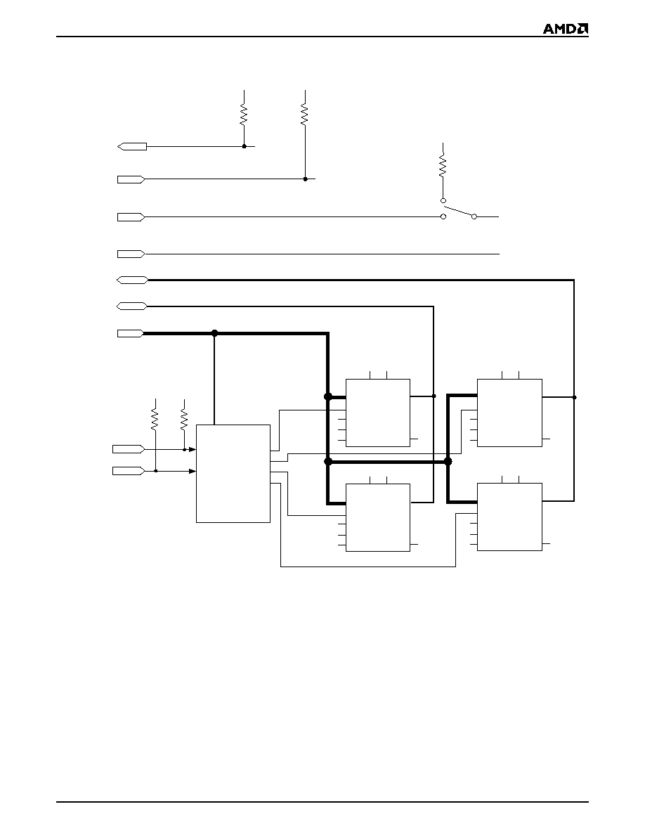
BLOCK DIAGRAM
*
4 Mbyte card only. Not used on 2 Mbyte card.
** 2 Mbyte card: Two Am29LV081 devices, S0 and S1
4 Mbyte card: Four Am29LV081 devices, S0...S3
Note: On the 2 Mbyte card, A20≠A24 are not connected. On the 4 Mbyte card, A21≠A24 are not connected. Connections not
shown in this diagram are not connected internally.
OE#
BUSY#
RY/BY#
A0-A20
Decoder*
CEL#
100K
100K
CEH#
WE#
WE# to all Flash devices
Write Protect
Switch
CEL0#
CEH0#
CEL1#
CEH1#
A20
V
CC
10K
V
CC
V
CC
OE# to all Flash devices
D0-D7
D8-D15
RESET#
RESET# to all Flash devices
A0-A19
CE#
WE#
OE#
D8-D15
V
SS
V
CC
RESET# RY/BY#
S1**
A0-A19
CE#
WE#
OE#
D0-D7
V
SS
V
CC
RESET# RY/BY#
S2**
A0-A19
CE#
WE#
OE#
D8-D15
V
SS
V
CC
RESET# RY/BY#
S3**
A0-A19
CE#
WE#
OE#
D0-D7
V
SS
V
CC
RESET# RY/BY#
S0**
V
CC
V
CC
100K
100K
21138E-2

6
AmMCL00XA
P R E L I M I N A R Y
MINIATURE CARD PAD ASSIGNMENTS
A0≠A24
Address A0 to A24 are the address bus lines that can
address up to 32 Mwords (64 Mbytes). The address
lines are word addressed. The Miniature Card specifi-
cation does not require the Miniature Card to decode
the upper address lines. A 2 Mbyte Miniature Card that
does not decode the upper address lines would repeat
its address space every 2 Mbytes. Address 0h would
access the same physical location as 200000h,
400000h, 600000h, etc. On the 2 Mbyte cards, A20≠
A24 are not connected. On the 4 Mbyte cards,
A21≠A24 are not connected.
D0≠D15
Data lines D0 through D15 constitute the data bus. The
data bus is composed of two bytes; the low byte is
D0≠D7 and the high byte is D8≠D15. These lines are
tristated when OE# is high.
OE#
OE# indicates to the card that the current bus cycle is
a read cycle. The output enable access time (t
OE
) is the
delay from the falling edge of OE# to valid data at the
output pins (assuming the addresses have been stable
for at least t
ACC
≠ t
OE
time).
WE#
WE# indicates to the card that the current bus cycle is
a write cycle. The falling edge of WE# (or CE#), which-
ever occurs later, latches address information and the
rising edge of WE# (or CE#), whichever occurs first
latches data/command information.
VS1#
Voltage Sense 1 signal. This signal is grounded.
VS2#
Voltage Sense 2 signal. This signal is left open or not
connected.
CEL#
CEL# enables the low byte of the data bus (D0≠D7) on
the card.
CEH#
CEH# enables the high byte of the data bus (D8≠D15)
on the card.
RESET#
RESET# controls card initialization. When RESET#
transitions from a low state to a high state, the Minia-
ture Card resets to the Read state after a maximum
delay of 20
µ
s.
BUSY#
BUSY# is a signal generated by the card to indicate the
status of operations within the Miniature Card. When
BUSY# is high, the Miniature Card is ready to accept
the next command from the host. When BUSY# is low,
the Miniature Card is busy and unable to accept most
data operations from the host. In Flash Miniature Cards
the BUSY# signal is tied to the components' RY/BY#
signal.
CD#
CD# is a grounded interface signal. After a Miniature
Card has been inserted, CD# will be forced low. The
card detect signal is located in the center of the second
row of interface signals, and should be one of the last
interface signals to connect to the host. Do not confuse
CD# with CINS#.
CINS#
CINS# is a grounded signal on the front of the Miniature
Card that is used for early detection of a card insertion.
CINS# makes contact on the host when the front of the
card is inserted into the socket, before the interface
signals connect.
BS8#
The BS8# (Bus size 8) signal indicates to the Minia-
ture Card that the host has an 8-bit bus. AMD Flash
Miniature Cards ignore this signal (no internal con-
nection). An 8-bit host must connect its D0≠D7 data
lines to D8≠D15 on the Miniature Card to retrieve the
upper (odd) byte.
GND
Ground
V
CC
Vcc is used to supply power to the card.
NC
No connect
RFU
Reserved for future use

AmMCL00XA 7
P R E L I M I N A R Y
ORDERING INFORMATION
Standard Products
AMD standard products are available in several packages and operating ranges. The order number (Valid Combination) is
formed by a combination of the following:
AM
MC
004
WP
SPEED OPTION
MINIATURE CARD
MEMORY CARD DENSITY
002
= 2 Megabyte Card
004
= 4 Megabyte Card
AMD
A
REVISION LEVEL
WRITE PROTECT SWITCH OPTION
WP
= Switch installed
-150
L
3 V, SINGLE SUPPLY OPERATION
2.7 V to 3.6 V, extended
operating voltage
I
TEMPERATURE RANGE
Blank = Commercial (0
∞
C to +70
∞
C)
I
= Industrial (≠40
∞
C to +85
∞
C)
8
AmMCL00XA
P R E L I M I N A R Y
INTERFACE SIGNAL ASSIGNMENTS
Note: NC = No Connect; RFU = Reserved for Future Use.
FLASH MINIATURE CARD OPERATIONS
Voltage Sensing
AMD Miniature Cards provide two voltage sense
signals for hosts that support multiple voltages. The
multivoltage host can sense the voltage level of the
Miniature Card and power up the card at that voltage.
S e e Ta b l e 3 f o r a d e s c r i p t i o n o f t h e v o l t a g e
sense signals.
In addition to the voltage sense pins, there are also
mechanical voltage keys on the Miniature Card that
ensure the card can only be inserted into host systems
that can supply the proper voltage levels to the card.
Refer to Section 4.1.2 in the Miniature Card specifica-
tion for more information on mechanical keying.
Table 3.
Voltage Sense Signals
Pad Number
Signal Name
Pad Number
Signal Name
Pad Number
Signal Name
1
A18
21
D12
41
A4
2
A16
22
D10
42
CEL#
3
A14
23
D9
43
A1
4
NC
24
D0
44
NC
5
CEH#
25
D2
45
NC
6
A11
26
D4
46
CD#
7
A9
27
RFU
47
A21
8
A8
28
D7
48
BUSY#
9
A6
29
NC
49
WE#
10
A5
30
NC
50
D14
11
A3
31
A19
51
RFU
12
A2
32
A17
52
D11
13
A0
33
A15
53
VS2#
14
NC
34
A13
54
D8
15
A24
35
A12
55
D1
16
A23
36
RESET#
56
D3
17
A22
37
A10
57
D5
18
OE#
38
VS1#
58
D6
19
D15
39
A7
59
RFU
20
D13
40
BS8#
60
A20
Miniature Card
Power-Up Voltage
VS1#
VS2#
3 volt-only
Gnd
Open
AmMCL00XA 9
P R E L I M I N A R Y
Data Accesses
The Miniature Card has a 16-bit data bus that can
accommodate word or byte accesses. By individually
asserting CEL# and CEH#, a host can access either
byte. However, byte swapping (moving the high byte
data to the low byte) is not supported.
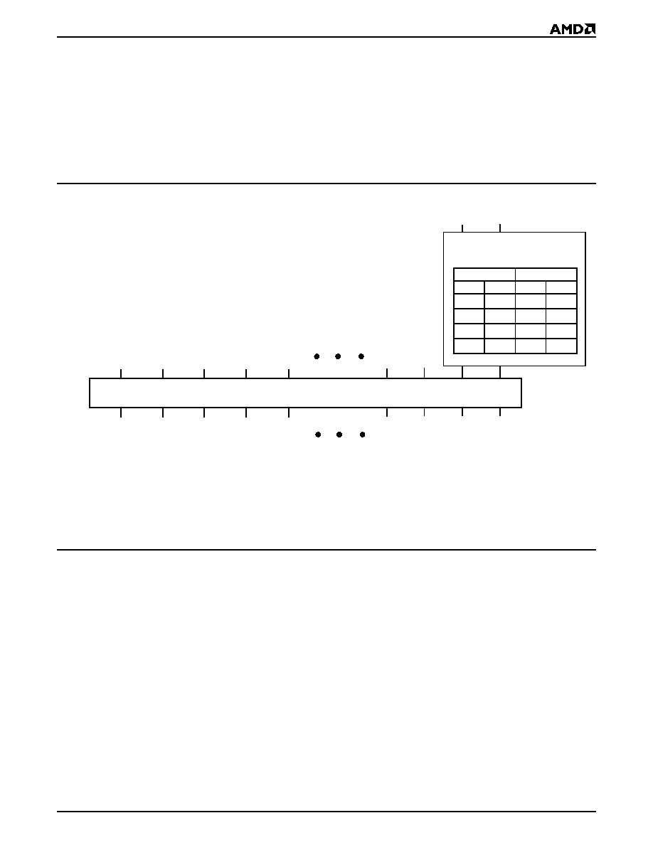
Figure 2 shows the connections between the host and
Miniature Card. The host system address lines range
from A0≠A25, whereas the Miniature Card address
lines range from A0≠A24. On the host, A0 and the
byte/word line are sent to a decoder and output to
CEL# and CEH# on the Miniature Card. These two bits
enable a single device for byte accesses and two
devices for word accesses, as shown by the decoder
truth table in Figure 2. Again, the Miniature Card
address lines do not receive input from host address bit
A0. In this document, all address references are
card
addresses
, unless otherwise noted. Table 4 shows the
read/write modes for Miniature Cards.
*
Not connected
**
Not connected on 2 Mbyte card
Figure 2.
Host/Card Address Connections
Word-Wide Operations
The AMD Miniature Card provide the flexibility to
operate on data in a byte-wide or word-wide format. In
word-wide operations, the low bytes are controlled with
CEL#. The high bytes are controlled with CEH#. Refer to
the block diagram for more information.
Byte-Wide Operations
Byte-wide data is available for read and write opera-
tions (CEL# = 0, CEH# = 1). Even and odd bytes are
stored in separate memory devices (for example, S0
and S1) and are accessed by controlling CEL# and
CEH#. The even byte is the low order byte and the odd
byte is the high order byte of a 16-bit word.
Each memory sector or device pair must be addressed
separately for erase operations. Refer to the block
diagram for more information.
Card Detection
Each CD# (output) pin should be detected by the host
system to determine if the memory card is adequately
seated in the socket. CD# and CINS# are internally tied
to ground. If both bits are not detected, the system
should indicate that the card must be re-inserted.
Data Protection
An optional mechanical write protect switch provides
user-initiated write protection. When this switch is acti-
vated,
WE#
is internally forced high. The Flash memory
command register is disabled from accepting any write
commands. This prevents the card from responding to
any commands (for example, an Autoselect com-
mand). See Figure 3.
Byte/Word
A0
A1
CEH#
CEL#
A0
A24
A23*
A24*
A23
A22*
A22
A21*
60-Pad Connector
A2
A1
Decoder
Decoder Truth Table
Input
Output
A0
B/W
CEL#
CEH#
0
0
0
0
0
1
0
1
1
0
0
0
1
1
1
0
A20**
A21
Card Bus
A25
21138E-3
Host Bus

10
AmMCL00XA
P R E L I M I N A R Y
Figure 3.
Write Protect Switch
(Card Right Side View)
In addition to card-level data protection, AMD Flash
Miniature Cards offer several device-level data protec-
tion features.
Device-Level Data Protection
AMD Flash memory devices offer protection against
accidental erasure or programming caused by spurious
system level signals that may exist during power tran-
sitions. During power up, each device automatically
resets the internal state machine to the read mode. The
control register architecture allows alteration of the
memory contents only occurs after successful comple-
tion of specific multi-bus cycle command sequences.
AMD Flash memory devices also incorporates the fol-
lowing features to prevent inadvertent write cycles
resulting from V
CC
power-up and power-down transi-
tions or system noise.
Low V
CC
Write Inhibit
To avoid initiation of a write cycle during V
CC
power-up
and power-down, the AMD memory devices in the Min-
iature Card lock out write cycles for V
CC
< V
LKO
(see
"DC Characteristics" on page 22 for voltages). When
V
CC
< V
LKO
, the command register is disabled, all
internal program/erase circuits are disabled, and the
device resets to the read mode. The memory devices
ignore all writes until V
CC
> V
LKO
. The user must
ensure that the control pins are in the correct logical
state when V
CC
> V
LKO
to prevent unintentional writes.
Write Pulse "Glitch" Protection
Noise pulses of less than 5 ns (typical) on OE#, CE#,
or WE# will neither initiate a write cycle nor change the
command registers.
Logical Inhibit
Writing is inhibited by holding any one of OE# = V
IL
,
CE# = V
IH
, or WE# = V
IH
. To initiate a write cycle CE#
and WE# must be a logical zero while OE# is a logical
one.
Power-Up Write Inhibit
Power-up of the device with CE# = WE# = V
IL
and OE#
= V
IH
will not accept commands on the rising edge of
WE#. The internal state machine is automatically reset
to the read mode on power-up.
Read Mode
Two Card Enable (CE#) pins are available on the
memory card. Both CE# pins must be active low for
word-wide read accesses. Only one CE# is required for
byte-wide accesses. The CE# pins select and deter-
mine when to apply power to the high-byte and
low-byte memory devices. The Output Enable (OE#)
controls gating accessed data from the memory device
outputs. Refer to Table 4.
The Miniature Card automatically powers up in the
read/reset state. In this case, a command sequence is
not required to read data. Standard microprocessor
read cycles will retrieve array data. This default state
ensures that no spurious alteration of the memory
content occurs during the power transition. Refer to the
AC Read Characteristics and Waveforms for the spe-
cific timing parameters.
Output Disable
Data outputs from the card are disabled when OE# is
at a logic-high level. Under this condition, outputs are
in the high-impedance state.
Write Enabled
Write Disabled
21138E-1

AmMCL00XA 11
P R E L I M I N A R Y
Table 4.
Miniature Card Read/Write Modes
Notes:
1. Unlisted access combinations are invalid and may return unexpected results.
2. X indicates a don't care value.
Erase Operations
The AMD Flash Miniature Card is organized as an
array of individual devices. Each Am29LV081 device
contains sixteen 64 KByte sectors, for a total of 1 Mbyte
of memory space per device.
Flash technology allows any logical "1" data bit to be pro-
grammed to a logical "0". The only way to reset bits to a
logical "1" is to erase that entire memory sector or
memory device. Once a memory sector or memory
device is erased, any address location may be pro-
grammed. Two or more devices may be erased concur-
rently when additional I
CC
current is supplied to the card.
However, erasing more than two devices concurrently is
not typical in battery-powered applications, but may take
place during procedures such as card testing.
Erase operations can be performed in several ways:
s
Erase a single sector or multiple sectors in a device
s
Erase a sector pair
s
Erase multiple device pairs*
s
Erase the entire card*
* This operation is only feasible in solutions capable of
supplying more than the specified miniature card
supply current requirement (150mA) per system. Each
AMD Flash memory device pair can accept a
maximum of 120mA supply current.
The common memory space data contents are altered
in a similar manner to writing to individual Flash
memory devices. An on-card address decoder acti-
vates the appropriate Flash device in the memory
array. Each device internally latches address and data
during write cycles. Refer to Table 4.
Standby Mode
The AMD flash devices are designed to accommodate
low standby power consumption. In order to achieve
standby mode, the CE# line must be deselected. In
addition, while in the standby mode, data I/O pins
remain in the high impedance state independent of the
voltage level applied to the OE# input. See the DC
Characteristics section for more details on Standby
Modes.
Deselecting CE# (CE# and RESET# = V
CC
±
0.3 V)
puts the device into the I
CC3
standby mode. If the
device is deselected during an Embedded Algorithm
operation, it continues to draw active power (I
CC2
) prior
to entering the standby mode, until the operation is
complete. When the device is again selected (CE# =
V
IL
), active operations occur in accordance with the
AC timing specifications.
Automatic Sleep Mode
Advanced power management features such as the
automatic sleep mode minimize Flash device energy
consumption. This is extremely important in bat-
tery-powered applications. The AMD memory devices
automatically enable the low-power, automatic sleep
mode when addresses remain stable for 300 ns. Auto-
matic sleep mode is independent of the CE#, WE#, and
OE# control signals. Typical sleep mode current draw
from each device is < 1
µ
A. Standard address access
timings provide new data when addresses are
Function
CEH#
CEL#
WE#
OE#
D8≠D15
D0≠D7
Read Mode
Word Access
L
L
H
L
High Byte Data
Low Byte Data
Low Byte Access
H
L
H
L
High-Z
Low Byte Data
High Byte Access
L
H
H
L
High Byte Data
High-Z
Write Mode
Word Access
L
L
L
H
High Byte Data
Low Byte Data
Low Byte Access
H
L
L
H
High-Z
Low Byte Data
High Byte Access
L
H
L
H
High Byte Data
High-Z
Standby Mode
Standby H
H
X
X
High-Z
High-Z

12
AmMCL00XA
P R E L I M I N A R Y
changed. While in sleep mode, output data is latched
and always available to the system.
Command Definitions
Each memory device contains a command register,
which is a latch that saves address, commands, and
data information used by the state machine and
memory array. The state machine is active when V
CC
is
greater than V
LKO
(2.3 - 2.5 V). This is required for valid
program and erase operations.
When Write Enable (WE#) and appropriate CE#
signals are at a logic-low level, and Output Enable
(OE#) is at a logic-high, the command register is
enabled for write operations. The falling edge of WE#
or CE#, whichever occurs later, latches address infor-
mation and the rising edge of WE# or CE#, whichever
occurs first, latches data/command information.
Commands are accomplished by writing non-specific
address and specific data sequences into the com-
mand register of accessed Flash memory devices.
Writing incorrect address and data values or writ-
ing them in the improper sequence will reset the
device to the read mode.
The byte-wide commands are defined in Tables 6 and
7; word-wide commands are defined in Table 5. Note
that the Erase Suspend (B0h) and Erase Resume
(30h) commands are valid only while the Sector Erase
operation is in progress.
Autoselect Operation
A host system or external card reader/writer can deter-
mine the on-card manufacturer and device I.D. codes.
Codes are available after writing the 90h command to
the command register of a memory device, as shown in
Tables 5 through 7. When the autoselect command is
issued to card address 00000h, the Miniature Card
returns the manufacturer I.D. If the autoselect
command is issued to card address 00001h, the Minia-
ture Card provides the device I.D.
To terminate the autoselect operation, the Read/Reset
command sequence must be written to the same
device. The Autoselect command operates only if the
card is not write protected.

AmMCL00XA 13
P R E L I M I N A R Y
Table 5.
Word Command Definitions
Legend:
X = Don't care
RA = Address of the memory location to be read.
RW = Data read from location RA during read operation.
PA = Address of the memory location to be programmed.
Addresses are latched on the falling edge of the WE# pulse.
PW = Data to be programmed at location PA. Data is latched
on the rising edge of WE#.
SA = Address of the sector to be erased. Refer to Table 8 for
sector addresses.
Notes:
1. Write protect must not be enabled for proper operation of
all commands. No command required for reading array
data, and can thus be done with write protect enabled.
2. During word addressing, CEL# = 0, CEH# = 0, and
address is applied to Memory Device Pair 0 (S0 and S1).
On 4 Mbyte cards, address for Memory Device Pair 1 =
(Addr) + 200000h, and address is applied to Memory
Device Pair 1 (S2 and S3). For host-to-card address bit
connections, see Figure 2.
3. All values are in hexadecimal.
4. The last bus cycle in an autoselect command sequence is
a read operation.
5. Word = high byte + low byte.
6. Address bits = X = Don't Care for all commands except for
Read Address (RA), Program Address (PA), and Sector
Address (SA).
7. The Erase Suspend command is valid only during a
sector erase operation. Refer to "Sector Erase Suspend".
8. The Erase Resume command is valid only during the
Erase Suspend mode.
9. See Table 4 for bus operations.
Embedded Command
Sequence (Note 1)
Bus Cycles (Notes 2≠9)
First
Second
Third
Fourth
Fifth
Sixth
Addr
Data
Addr
Data
Addr
Data
Addr
Data
Addr
Data
Addr
Data
Read
1
RA
RW
Reset
1
XXXX
F0F0
Autoselect Manufacturer ID
(Note 4)
4
XXXX
AAAA
XXXX
5555
XXXX
9090
XX00
0101
Autoselect Device ID
(Note 4)
4
XXXX
AAAA
XXXX
5555
XXXX
9090
XX01
3838
Word Write
4
XXXX
AAAA
XXXX
5555
XXXX
A0A0
PA
PW
Device Erase
6
XXXX
AAAA
XXXX
5555
XXXX
8080
XXXX
AAAA
XXXX
5555
XXXX
1010
Sector Erase
6
XXXX
AAAA
XXXX
5555
XXXX
8080
XXXX
AAAA
XXXX
5555
SA
3030
Sector Erase Suspend (Note 7)
1
XXXX
B0B0
Sector Erase Resume (Note 8)
1
XXXX
3030
C
ycl
es

14
AmMCL00XA
P R E L I M I N A R Y
Table 6.
Even Byte Command Definitions
Note for Table 6: During even (low) byte accesses, CEL# = 0, CEH# = 1. Address is applied to Memory Device 0 (S0). On 4 Mbyte
cards, address for Memory Device 2 (S2) = (Addr) + 200000h.
Table 7.
Odd
Byte Command Definitions
Note for Table 7: During odd (high) byte accesses, CEL#= 1, CEH# = 0, and address is applied to Memory Device 1 (S1). On 4 Mbyte
cards, address for Memory Device 3 (S3) = (Addr) + 200000h + 100000h.
Legend for Tables 6 and 7:
X = Don't care
RA = Address of the memory location to be read.
RW = Data read from location RA during read operation.
PA = Address of the memory location to be programmed.
Addresses are latched on the falling edge of the WE# pulse.
PW = Data to be programmed at location PA. Data is latched on
the rising edge of WE#.
SA = Address of the sector to be erased. Refer to Table 8 for
sector addresses.
Notes for Tables 6 and 7:
1. Write protect must not be enabled for proper operation of all
commands. No command required for reading array data,
and can thus be done with write protect enabled.
2. For host-to-card address bit connections, see Figure 2.
3. All values are in hexadecimal.
4. The last bus cycle in an autoselect command sequence is a
read operation.
5. Address bits = X = Don't Care for all commands except for
Read Address (RA), Program Address (PA), and Sector
Address (SA).
6. The Erase Suspend command is valid only during a sector
erase operation. Refer to "Sector Erase Suspend".
7. The Erase Resume command is valid only during the Erase
Suspend mode.
8. See Table 4 for bus operations.
Embedded Command Sequence
(Note 1)
Bus Cycles (Notes 2≠8)
First
Second
Third
Fourth
Fifth
Sixth
Addr
Data
Addr
Data
Addr
Data
Addr
Data
Addr
Data
Addr
Data
Read
1
RA
RD
Reset
1
XXXX XXF0
Autoselect Manufacturer ID (Note 4)
4
XXXX
XXAA
XXXX
XX55
XXXX
XX90
XX00
XX01
Device ID (Note 4)
4
XXXX
XXAA
XXXX
XX55
XXXX
XX90
XX01
XX38
Byte Write
4
XXXX
XXAA
XXXX
XX55
XXXX
XXA0
PA
PD
Device Erase
6
XXXX
XXAA
XXXX
XX55
XXXX
XX80
XXXX
XXAA
XXXX
XX55
XXXX
XX10
Sector Erase
6
XXXX
XXAA
XXXX
XX55
XXXX
XX80
XXXX
XXAA
XXXX
XX55
SA
XX30
Sector Erase Suspend (Note 6)
1
XXXX XXB0
Sector Erase Resume (Note 7)
1
XXXX XX30
Embedded Command Sequence
(Note 1)
Bus Cycles (Notes 2≠8)
First
Second
Third
Fourth
Fifth
Sixth
Addr
Data
Addr
Data
Addr
Data
Addr
Data
Addr
Data
Addr
Data
Read
1
RA
RD
Reset
1
XXXX XXF0
Autoselect Manufacturer ID (Note 4)
4
XXXX
AAXX
XXXX
55XX
XXXX
90XX
XX00
01XX
Autoselect Device ID (Note 4)
4
XXXX
AAXX
XXXX
55XX
XXXX
90XX
XX01
38XX
Byte Write
4
XXXX
AAXX
XXXX
55XX
XXXX
A0XX
PA
PDXX
Device Erase
6
XXXX
AAXX
XXXX
55XX
XXXX
80XX
XXXX
AAXX
XXXX
55XX
XXXX
10XX
Sector Erase
6
XXXX
AAXX
XXXX
55XX
XXXX
80XX
XXXX
AAXX
XXXX
55XX
SA
30XX
Sector Erase Suspend (Note 6)
1
XXXX XXB0
Sector Erase Resume (Note 7)
1
XXXX XX30
Cy
c
l
e
s
Cy
c
l
e
s

AmMCL00XA 15
P R E L I M I N A R Y
Table 8.
Memory Sector Addresses
Notes:
1. For word addressing, devices 0 and 1 (S0 and S1) together form Memory Device Pair 0; devices 2 and 3 (S2 and S3) form
Memory Device Pair 1. Refer to the block diagram for device connections.
2. Card address bits range from A0 to A19. Host address bits range from A0 to A20. Host address bit A0 is used for controlling
the CEL# and CEH# inputs to the card. Refer to Figure 2 for host-to-card address bit connections.
Sector
Card Address Bits
Device 0 and/or 1 (Note 1)
Device 2 and/or 3 (Note 1)
A19
A18
A17
A16
Card Address Range
Card Address Range
0
0
0
0
0
00000h≠0FFFFh
100000h≠10FFFFh
1
0
0
0
1
10000h≠1FFFFh
110000h≠11FFFFh
2
0
0
1
0
20000h≠2FFFFh
120000h≠12FFFFh
3
0
0
1
1
30000h≠3FFFFh
130000h≠13FFFFh
4
0
1
0
0
40000h≠4FFFFh
140000h≠14FFFFh
5
0
1
0
1
50000h≠5FFFFh
150000h≠15FFFFh
6
0
1
1
0
60000h≠6FFFFh
160000h≠16FFFFh
7
0
1
1
1
70000h≠7FFFFh
170000h≠17FFFFh
8
1
0
0
0
80000h≠8FFFFh
180000h≠18FFFFh
9
1
0
0
1
90000h≠9FFFFh
190000h≠19FFFFh
10
1
0
1
0
A0000h≠AFFFFh
1A0000h≠1AFFFFh
11
1
0
1
1
B0000h≠BFFFFh
1B0000h≠1BFFFFh
12
1
1
0
0
C0000h≠CFFFFh
1C0000h≠1CFFFFh
13
1
1
0
1
D0000h≠DFFFFh
1D0000h≠1DFFFFh
14
1
1
1
0
E0000h≠EFFFFh
1E0000h≠1EFFFFh
15
1
1
1
1
F0000h≠FFFFFh
1F0000h≠1FFFFFh

16
AmMCL00XA
P R E L I M I N A R Y
AMD FLASH MEMORY PROGRAM AND
ERASE OPERATIONS
To simplify program and erase operations, AMD Flash
Memory devices include Embedded Algorithms
(Embedded Erase Algorithm and Embedded Program
Algorithm) that allow the host to simply issue a com-
mand, after which it is free to perform other tasks. The
host then only needs to monitor appropriate status bits
to determine when the operation is complete.
Embedded Erase Algorithm
When erasing a sector or device, the Embedded Erase
algorithm does not require the host to first entirely
p r e - p r o g r a m t h e d e v i c e . U p o n e x e c u t in g t h e
Embedded Erase command sequence, the addressed
memory sector or memory device automatically writes
and verifies the entire memory device or memory
sector for an all "0" data pattern. The system is not
required to provide any controls or timing during these
operations.
When the memory sector or memory device is auto-
matically verified to contain an all "0" pattern, a
self-timed chip erase-and-verify begins. The erase and
verify operations are complete when the data on D7
(D15 on the odd byte) of the memory sector or memory
device is "1" (see Write Operation Status section), at
which time the device returns to the read mode. The
system is not required to provide any control or timing
during these operations. If a Reset command is issued
while the erase operation is in progress, the erase
operation will stop, and the data in that device will be
undefined. In that case, restart the erase on that sector
a n d a l l o w i t t o c o m p l e t e .
When using the Embedded Erase algorithm, the erase
automatically terminates when adequate erase margin
has been achieved for the memory array (no erase
verify command is required).
The Embedded Erase command sequence is a
command only operation that stages the memory
sector or memory device for automatic electrical
erasure of all bytes in the array. The automatic erase
begins on the rising edge of the
WE#
and terminates
when the data on D7 (D15 on the odd byte) of the
memory sector or memory device is "1" (see Write
Operation Status section) at which time the device
returns to the Read mode. Please note that for the
memory device or memory sector erase operation,
Data Polling may be performed at any address in that
device or sector.
Figure 4 and Table 9 illustrate the Embedded Erase
Algorithm, a typical command string and bus operations.
As described earlier, once the memory sector in a
device or memory device completes the Embedded
Erase operation, it returns to the Read mode and
addresses are no longer latched. Therefore, the device
requires that a valid address input to the device is
supplied by the system at this particular instant of time.
Otherwise, the system will never read a "1" on D7 (D15
on the odd byte). A system designer has the following
choices to implement the Embedded Erase algorithm:
1. The host may keep the sector address (within any
of the sectors being erased) valid during the entire
Embedded Erase operation.
2. Once the system executes the Embedded Erase
command sequence, the host may remove the ad-
dress from the device and perform other tasks. The
host is required to keep track of the valid sector ad-
dress by loading it into a temporary register. When
the host comes back to Data Poll the device, it must
reassert the same address.
3. The host may monitor BUSY# (RY/BY#) to deter-
mine the status of the Embedded Algorithm in
progress. A "0" indicates that the device is busy; a
"1" indicates that the algorithm is complete.
Sector Erase
Sector erase is a six bus cycle operation. There are two
"unlock" write cycles. These are followed by writing the
"set-up" command. Two more "unlock" write cycles are
then followed by the sector erase command. The
sector address (any address location within the desired
sector) is latched on the falling edge of WE# (or CE#),
whichever occurs later, while the data is latched on the
rising edge of WE# (or CE#) pulse, whichever occurs
first. A time-out of 80
µ
s from the rising edge of the last
sector erase command will initiate the sector erase
c o m m a n d .
Multiple sectors can be specified for erase by writing
the six bus cycle operation as described above and
then following it by additional writes of the Sector Erase
command to addresses of other sectors to be erased.
The time between Sector Erase command writes must
be less than 80
µ
s, otherwise that command will not be
accepted. It is recommended that processor interrupts
be disabled during this time to guarantee this condition.
The interrupts can be re-enabled after the last Sector
Erase command is written. A time-out of 80
µ
s from the
rising edge of the last WE# (or CE#) will initiate the ex-
ecution of the Sector Erase command(s). If another
falling edge of the WE# (or CE#) occurs within the 80
µ
s time-out window, the timer is reset. During the 80
µ
s
window, any command other than Sector Erase or
Erase Suspend written to the device will reset the de-
vice back to Read mode. Once the 80
µ
s window has
timed out, only the Erase suspend command is recog-
nized. Note that although the Reset command is not
recognized in the Erase Suspend mode, the device is
available for read or program operations in sectors that
are not erase suspended. The Erase Suspended and
Erase Resume commands may be written as often as
required during a sector erase operation. Hence, once
erase has begun, it must ultimately complete unless

AmMCL00XA 17
P R E L I M I N A R Y
Hardware Reset is initiated. Loading the sector erase
registers may be done in any sequence and with any
number of sectors (0 to 15).
A Reset command issued after the device has begun
execution stops the erase operation, but the data in the
sector will be undefined. In that case, restart the erase
on that sector and allow it to complete.
The automatic sector erase begins after the 80
µ
s time
out from the rising edge of the
WE#
(or
CE#
) pulse for
the last sector erase command pulse and terminates
when the data on D7 is "1" (see Write Operation Status
section) at which time the device returns to read mode.
Data Polling must be performed at an address within
any of the sectors being erased.
If DATA Polling or the Toggle Bit indicates the device
has been written with a valid Sector Erase command,
D3 may be used to determine if the sector erase timer
window is still open. If D3 is high (`1'), the internally
controlled erase cycle has begun; attempts to write
subsequent commands to the device will be ignored
until the erase operation is completed as indicated by
the DATA Polling or Toggle Bit. If D3 is low (`0'), the
device will accept additional sector erase commands.
To be certain the command has been accepted, the
software should check the status of D3 following each
Sector Erase command. If D3 was high on the second
status check, the command may not have been
accepted.
It is recommended that the user guarantee the time
between sector erase command writes be less than 80
µ
s by disabling the processor interrupts just for the
duration of the Sector Erase (30H) commands. This
approach will ensure that sequential sector erase
command writes will be written to the device while the
sector erase timer window is still open.
Figure 4 illustrates the Embedded Erase Algorithm
using typical command strings and bus operations.
Table 9.
Embedded Erase Algorithm
Figure 4.
Embedded Erase Algorithm
Note: The latest release of the software drivers for AMD
Miniature Cards and devices may be downloaded from the
AMD web site at http://www.amd.com.
Embedded Program Algorithm
The Embedded Program setup is a four bus cycle oper-
ation that stages the addressed memory location or
memory device for automatic programming.
Once the Embedded Program setup operation is per-
formed, the next
WE#
pulse causes a transition to an
active programming operation. Addresses are inter-
nally latched on the falling edge of the
WE#
(or
CE#
)
pulse. Data is internally latched on the rising edge of
the
WE#
pulse. The rising edge of
WE#
also begins the
programming operation. The system is not required to
provide further control or timing. The device will auto-
matically provide an adequate internally generated
write pulse and verify margin. The automatic program-
ming operation is completed when the data on D7 of
the addressed memory sector or memory device is
equivalent to data written to this bit (see Write Opera-
tion Status section) at which time the device returns to
the Read mode (no write verify command is required).
Addresses are latched on the falling edge of
WE#
(or
CE#
)
during the Embedded Program command execu-
tion and hence the system is not required to keep the
addresses stable during the entire Programming opera-
tion. However, once the device comple te s the
Embedded Program operation, it returns to the Read
mode and addresses are no longer latched. Since a
verify valid data must occur on D7, at this particular
instant, the system is required to supply a valid address
input to the device. A system designer has three choices
to implement the Embedded Programming algorithm:
Bus
Operation
Command
Comments
Standby
Wait for V
CC
ramp
Write
Embedded Erase
command sequence
6 bus cycle operation
Read
Data Poll or check
BUSY# (RY/BY#)
to verify erasure
Write Embedded Erase
Command Sequence
(See Tables 5≠7)
Data
Poll from Device
or wait for BUSY#
(RY/BY#)
Start
Erasure Complete
21138E-5

18
AmMCL00XA
P R E L I M I N A R Y
1. The system (CPU) keeps the address valid during
the entire Embedded Programming operation, or
2. Once the system executes the Embedded Pro-
gramming command sequence, the CPU takes
away the address from the device and becomes
free to do other tasks. In this case, the CPU is re-
quired to keep track of the valid address by loading
it into a temporary register. When the CPU comes
back for performing Data Polling, it should reassert
t h e s a m e a d d r e s s .
3. The host may monitor BUSY# (RY/BY#) to deter-
mine the status of the Embedded Algorithm in
progress. A "0" indicates that the device is busy; a
"1" indicates that the algorithm is complete.
However, since the Embedded Programming operation
takes only 9
µ
s typically, it may be easier for the CPU
to keep the address stable during the entire Embedded
Programming operation instead of reasserting the valid
address during Data Polling. Any commands written to
the device during this period will be ignored. Figure 5
and Table 10 illustrate the Embedded Program Algo-
rithm, a typical command string, and bus operation.
Table 10.
Embedded Program Algorithm
Figure 5.
Embedded Program Algorithm
Reset Command
The device will automatically power up in the read/re-
set state. In this case, a command sequence is not re-
quired to read data. Standard microprocessor cycles
will retrieve array data. This default value ensures that
no spurious alteration of the memory content occurs
during the power transition. Refer to the AC Character-
istics section for the specific timing parameters.
The reset operation is initiated by writing the read/reset
command sequence into the command register. Micro-
processor read cycles retrieve array data from the
memory. The device remains enabled for reads until
the command register contents are altered.
Sector Erase Suspend
The Erase Suspend command allows the user to inter-
rupt a Sector Erase operation and then perform data
read or programs in a sector not being erased. This
command is applicable only during the Sector Erase
operation, which includes the time-out period for Sector
Erase. The Erase Suspend command will be ignored if
written during the execution of the Chip Erase opera-
tion or Embedded Program Algorithm (but will reset the
chip if written improperly during the command se-
quences.) Writing the Erase Suspend command during
the Sector Erase time-out results in immediate termina-
tion of the time-out period and suspension of the erase
operation. Once in Erase Suspend, the device is avail-
Bus
Operation
Command
Comments
Standby
Wait for V
CC
ramp
Write
Embedded Program
command sequence
3 bus cycle operation
Write
Program
Address/Data
1 bus cycle operation
Read
Data
Poll or check
BUSY# (RY/BY#) to
verify program
21138E-6
Write Embedded Write Command
Sequence per Tables 5≠7
Verify
Data
N
Y
Data
Poll Device
or wait for BUSY# (RY/BY#)
Y
Increment
Address
N
Start
Completed
Last
Address

AmMCL00XA 19
P R E L I M I N A R Y
able for read (note that in the Erase Suspend mode, the
Reset/Read command is not required for read opera-
tions and is ignored) or program operations in sectors
not being erased. Any other command written during
the Erase Suspend mode will be ignored, except for the
Erase Resume command. Writing the Erase Resume
command resumes the sector erase operation. The ad-
dresses are "don't cares" when writing the Erase Sus-
pend or Erase Resume command.
When the Erase Suspend command is written during a
Sector Erase operation, the chip will take between 0.1
µ
s and 20
µ
s to actually suspend the operation and go
into erase suspended read mode (pseudo-read mode),
at which time the user can read or program from a sec-
tor that is not erase suspended. Reading data in this
mode is the same as reading from the standard read
mode, except that the data must be read from sectors
that have not been erase suspended.
Successively reading from the erase-suspended sec-
tor while the device is in the erase-suspend-read mode
will cause D2 to toggle. Polling D2 on successive reads
from a given sector provides the system the ability to
determine if a sector is in Erase Suspend.
After entering the erase-suspend-read mode, the user
can program the device by writing the appropriate com-
mand sequence for Byte Program. This program mode
is known as the erase suspend-program mode. Again,
programming in this mode is the same as programming
in the regular Byte Program mode, except that the data
must be programmed to sectors that are not erase sus-
pended. Successively reading from the erase sus-
pended sector while the device is in the erase
suspend-program mode will cause D2 to toggle. Com-
pletion of the erase suspend operation can be deter-
mined two ways:
s
Checking the status of the toggle bit D2
s
Checking the status of the RY/BY# pin
To resume the operation of Sector Erase, the Resume
command (30H) should be written. Any further writes of
the Resume command at this point will be ignored.
However, another Erase Suspend command can be
written after the device has resumed sector erase op-
erations.
Write Operation Status
Table 11 shows the status bit states for device program
and erase operations.
Data Polling--D7 (D15 on Odd Byte)
The Miniature card features DATA Polling as a method
to indicate to the host system that the embedded algo-
rithms are in progress or completed.
During the Embedded Program Algorithm, an attempt
to read the device will produce the compliment of the
data last written to D7. Upon completion of the Embed-
ded Program Algorithm, an attempt to read the device
will produce the true data last written to D7. Note that
just at the instant when D7 switches to true data, the
other bits, D6≠D0, may not yet be true data. However,
they will all be true data on the next read from the de-
vice. Please note that Data Polling (D7) may give an
inaccurate result when an attempt is made to write
to a protected sector. During an Embedded Erase Al-
gorithm, an attempt to read the device will produce a `0'
at the D7 output. Upon completion of the Embedded
E r a s e A l g o r i t h m , a n a t t e m p t t o r e a d
the device will produce a `1' at D7.
Note: D7 is rechecked even if D5 = 1 because D7 may
change simultaneously with D5.
Figure 6.
Data Polling Algorithm
START
DQ7 = Data?
Yes
No
No
DQ5 = 1?
No
Yes
DQ7 = Data?
Yes
FAIL
PASS
21138E-7

20
AmMCL00XA
P R E L I M I N A R Y
Table 11.
Hardware Sequence Flags
Notes:
1. Performing successive read operations from the erase-suspended sector will cause D2 to toggle.
2. Performing successive read operations from any address will cause D6 to toggle.
3. Reading the byte address being programmed while in the erase-suspend program mode will indicate logic "1" at the D2 bit.
However, successive reads from the erase-suspended sector will cause D2 to toggle.
BUSY# (RY/BY#--Ready/Busy)
The BUSY# signal indicates to the host the status of
operations within the Miniature Card. The BUSY#
signal is tied to the components' RY/BY# pins.
The RY/BY# signal from AMD Flash devices in
the Miniature Card indicate that the Embedded Algo-
rithms are either in progress or have been completed.
If the output is low, the device is busy with either a
program or erase operation. If the output is high, the
device is ready to accept any read/write or erase op-
eration. When the RY/BY# pin is low, the device will
not accept any additional program or erase com-
mands with the exception of the Erase Suspend com-
mand. If a Flash device is placed in an Erase
Suspend mode, the RY/BY# output will be high. Refer
to the section "Sector Erase Suspend" for more infor-
mation.
WORD-WIDE PROGRAMMING
The Word-Wide Programming sequence will be as
usual per Table 5. The Program word command is
A0A0H. Each byte is independently programmed. For
example, if the high byte of the word indicates
the successful completion of programming via one of
its write status bits such as D15, software polling
should continue to monitor the low byte for write com-
pletion and data verification, or vice versa. During the
Embedded Programming operations the device exe-
cutes programming pulses in 9
µ
s increments.
WORD-WIDE SECTOR ERASING
The Word-Wide Sector Erasing of a memory device
pair is similar to word-wide programming. The erase
word command is a six-bus-cycle command sequence
(see Table 5). Each sector is independently erased and
verified. Word-wide erasure reduces total erase time
when compared to byte erasure. Each Flash memory
device in the card may erase at different rates. There-
fore, each device (byte) must be verified separately.
Status
D7
D6
D5
D3
D2
In Progress
Byte Program in Embedded Program Algorithm
D7
Toggle
0
0
1
Embedded Erase Algorithm
0
Toggle
0
1
Toggle
Erase Suspended Mode
Erase Suspend Read
(Erase Suspended Sector)
1
1
0
0
Toggle
(Note 1)
Erase Suspend Read
(Non-Erase Suspended Sector)
Data
Data
Data
Data
Data
Erase Suspend Program
(Non-Erase Suspended Sector)
D7
Toggle
(Note 2)
0
1
1
(Note 3)
Exceeded
Time Limits
Byte Program in Embedded Program Algorithm
D7
Toggle
1
0
1
Program/Erase in Embedded Erase Algorithm
0
Toggle
1
1
N/A
Erase Suspended Mode
Erase Suspend Program
(Non-Erase Suspended Sector)
D7
Toggle
1
1
N/A

AmMCL00XA 21
P R E L I M I N A R Y
ABSOLUTE MAXIMUM RATINGS
Storage Temperature . . . . . . . . . . . . . ≠40
∞
C to +90
∞
C
Ambient Temperature
with Power Applied . . . . . . . . . . . . . . ≠40
∞
C to +85
∞
C
Voltage at All Pins (Note 1) . . . . ≠0.5 V to V
CC
+0.5 V
V
CC
(Note 1) . . . . . . . . . . . . . . . . . . . . ≠0.5 V to 3.6 V
Output Short Circuit Current (Note 2) . . . . . . 200 mA
Notes:
1. Minimum DC voltage on input or I/O pins is ≠0.5 V. During
voltage transitions, inputs may overshoot V
SS
to ≠2.0 V
for periods of up to 20 ns. Maximum DC voltage on output
and I/O pins is V
CC
+ 0.5 V. During voltage transitions,
outputs may overshoot to V
CC
+ 2.0 V for periods up to
20ns.
2. No more than one output shorted at a time. Duration of
the short circuit should not be greater than one second.
Conditions equal V
OUT
= 0.5 V or 3.6 V, V
CC
= V
CCmax
.
These values are chosen to avoid test problems caused
by tester ground degradation. This parameter is sampled
and not 100% tested, but guaranteed by characterization.
3. Stresses above those listed under "Absolute Maximum
Ratings" may cause permanent damage to the device.
This is a stress rating only; functional operation of the de-
vice at these or any other conditions above those indi-
cated in the operational sections of this specification is
not implied. Exposure of the device to absolute maximum
rating conditions for extended periods may affect device
reliability.
OPERATING RANGES
Commercial Devices
Case Temperature (T
C
). . . . . . . . . . . . . .0
∞
C to +70
∞
C
Industrial (I) Devices
Case Temperature (T
C
). . . . . . . . . . . .≠40
∞
C to +85
∞
C
V
CC
Supply Voltages
AmMCL00XAWP-150 . . . . . . . . . . . . +2.7 V to +3.6 V
Operating ranges define those limits between which the
functionality of the device is guaranteed.

22
AmMCL00XA
P R E L I M I N A R Y
DC CHARACTERISTICS
Notes:
1. V
CC
= 2.7 V to 3.6 V.
2. Supply current is a max RMS value. Read frequency = 5
MHz.
CONNECTOR DC SPECIFICATIONS
Notes:
1. This current is a minimum that the connector should withstand, and a maximum that the host should provide.
2. On the host, these specifications must be met for one conducting channel on elastomeric connectors.
CARD AND PAD CAPACITANCE
Notes:
1. Sampled, not 100% tested.
2. Test conditions T
A
= 25
∞
C, f = 1.0 MHz.
Parameter
Symbol
Parameter Description
Test Conditions
Min
Max
Unit
I
LI
Input Leakage Current
V
IN
= V
SS
to V
CC,
V
CC
= V
CC max
±
5
µ
A
I
LO
Output Leakage Current
V
IN
= V
SS
to V
CC,
V
CC
= V
CC max
±
5
µ
A
I
CCS
V
CC
Standby Current
CEL#, CEH#, RESET# = V
CC
± 0.3
V
V
CC
= 3.6V; V
IN
= V
SS
or V
CC
2 Mbyte
30
µ
A
4 Mbyte
40
µ
A
I
CC
V
CC
Supply Current, word
mode (Note 2)
RESET# = V
IH
; CEL# and CEH# =
V
IL
Read
40
mA
Write
60
mA
V
IL
Input Low Voltage
≠0.5
0.8
V
V
IH
Input High Voltage
0.7 V
CC
V
CC
+ 0.5
V
V
OL
Output Low Voltage
I
OUT
= 5.8 mA
0.45
V
V
OH
Output High Voltage
I
OUT
= ≠2.0 mA
0.85 V
CC
V
V
LKO
Low V
CC
Lock-Out Voltage
2.3
2.5
V
Parameter Min
Max
Units
Interface Signal Resistance (Note 2)
2.0
Interface Signal Current (Notes 1, 2)
125
mA
Power/Insertion Signal Resistance
0.060
Power/Insertion Signal Current (Note 1)
500
mA
Parameter Symbol
Parameter Description
Test Conditions
Max
Unit
C
CARD
Card Input Capacitance
40
pF
C
HOST
System Load Capacitance
120
pF
C
I/O
I/O
Capacitance
D0-D15
40
pF

AmMCL00XA 23
P R E L I M I N A R Y
AC CHARACTERISTICS
Read-only Operations
Parameter Symbol
Parameter Description
-150
Unit
JEDEC
Standard
t
AVAV
t
RC
Read Cycle Time
Min
150
ns
t
ELQV
t
CE
Chip Enable Access Time
Max
150
ns
t
AVQV
t
ACC
Address Access Time
Max
150
ns
t
GLQV
t
OE
Output Enable Access Time
Max
50
ns
t
ELQX
t
LZ
Chip Enable to Output in Low-Z
Min
5
ns
t
EHQZ
t
DF
Chip Disable to Output in High-Z
Max
30
ns
t
GLQX
t
OLZ
Output Enable to Output in Low-Z
Min
5
ns
t
GHQZ
t
DF
Output Disable to Output in High-Z
Max
30
ns
t
AXQX
t
OH
Output Hold from First of Address, CE#,
or
OE#
Change
Min
5
ns
t
Ready
RESET# Pin Low to Read Mode
Max
20
µ
s
24
AmMCL00XA
P R E L I M I N A R Y
AC CHARACTERISTICS
Write Operations (Erase/Program)
Parameter Symbols
Parameter Description
-150
Unit
JEDEC
Standard
t
AVAV
t
WC
Write Cycle Time
Min
150
ns
t
WLWH
WE# pulse width
Min
50
ns
t
ELGL
t
ELWL
CE# setup time to WE# or OE# active
Min
0
ns
t
AVGL
t
AVWL
Address setup time to WE# or OE# active
Min
0
ns
t
DVWH
Data setup time to WE# inactive
Min
50
ns
t
WHDX
Data hold time from WE# inactive
Min
0
ns
t
WHAX
Address hold time from WE# inactive
Min
0
ns
t
WHEH
CE# hold time from WE# inactive
Min
0
ns
t
RP
RESET# Pulse Width
Min
500
ns
t
BUSY
Program/Erase Valid to RY/BY# Delay
Min
90
ns
t
WHWH1
Programming Operation
Typ
9
Max
300
µ
s
t
WHWH2
Sector Erase Operation
Typ
1.5
Max
15
s

AmMCL00XA 25
P R E L I M I N A R Y
KEY TO SWITCHING WAVEFORMS
SWITCHING WAVEFORMS
Figure 7.
AC Waveforms for Read Operations
Must be
Steady
May
Change
from H to L
May
Change
from L to H
Does Not
Apply
Don't Care,
Any Change
Permitted
Will be
Steady
Will be
Changing
from H to L
Will be
Changing
from L to H
Changing,
State
Unknown
Center
Line is High-
Impedance
"Off" State
WAVEFORM
INPUTS
OUTPUTS
KS000010
t
AVAV
t
AVQV
t
AVGL
t
EHQX
OE#
CEL#/CEH#
D0≠D15
Valid Data
t
ELGL
t
ELQV
t
ELQNZ
t
GHQZ
t
AXQX
t
GHQX
t
GLQNZ
t
GLQV
A0≠A25
21138E-8

26
AmMCL00XA
P R E L I M I N A R Y
SWITCHING WAVEFORMS
Figure 8.
AC Waveforms for Write Operations
Figure 9.
AC Waveforms for Data Polling During Embedded Algorithm Operations
t
AVAV
WE#
CEL#/CEH#
D0≠D15
t
DVWH
A0≠A25
t
WLWH
t
AVWL
t
WHEH
t
WHAX
t
WHDX
Valid Data
t
ELWL
21138E-9
D0≠D7
Valid Data
t
CH
t
OEH
t
OE
t
CE
t
WHWH1 or
t
WHWH2
D7=
Valid Data
High Z
CE#
OE#
WE#
t
OH
D7#
D0≠D6=Invalid
*D7=Valid Data (The device has completed the Embedded operation).
*
21138E-10
D0≠D6
t
DF
D7

AmMCL00XA 27
P R E L I M I N A R Y
SWITCHING WAVEFORMS
Figure 10.
RY/BY# Timing Diagram During Program/Erase Operations
Figure 11.
RESET# Timing Diagram
CE#
WE#
RY/BY#
t
BUSY
Entire programming
or erase operations
The rising edge of the last WE# signal
21138E-11
RESET#
21138E-12
t
Ready
t
RP

28
AmMCL00XA
P R E L I M I N A R Y
AC CHARACTERISTICS-ALTERNATE CE# CONTROLLED WRITES
Write/Erase/Program Operations
Notes:
1. Rise/fall time
10 ns.
2. Maximum specification not needed due to the internal stop timer that will stop any erase or write operation that exceed the
device specification.
3. Card Enable Controlled Programming:
Flash Programming is controlled by the valid combination of the Card Enable (CE1#, CE2#) and Write Enable (WE#) signals.
For systems that use the Card Enable signal(s) to define the write pulse width, all setup, hold, and inactive write enable timing
should be measured relative to the Card Enable signal(s).
4. Under worst case condition of 90
∞
C, Vcc = 2.7 V, 100,000 cycles. Excludes system level overhead, the time required to
execute the four bus cycle command necessary to program each byte.
Parameter Symbols
Parameter Description
-150
Unit
JEDEC
Standard
tAVAV
tWC
Write Cycle Time
Min
150
ns
tAVEL
tAS
Address Setup Time
Min
10
ns
tELAX
tAH
Address Hold Time
Min
50
ns
tDVEH
tDS
Data Setup Time
Min
50
ns
tEHDX
tDH
Data Hold Time
Min
0
ns
tGLDV
tOEH
Output Enable Hold Time for Embedded Algorithm
Min
10
ns
tGHEL
Read Recovery Time before Write
Min
0
µ
s
tWLEL
tWS
WE# Setup Time before CE#
Min
0
ns
tEHWH
tWH
WE# Hold Time
Min
0
ns
tELEH
tCP
CE# Pulse Width
Min
50
ns
tEHEL
tCPH
CE# Pulse Width HIGH (Note 3)
Min
20
ns
tEHEH3
Embedded Programming Operation (Notes 3,4)
Typ
9
Max
300
µ
s
tEHEH4
Embedded Erase Operation for each 64K byte Memory
Sector (Notes 1, 2)
Typ
1.5
Max
15
s
tVCS
VCC Setup Time to Write Enable LOW
Min
50
µ
s
AmMCL00XA 29
P R E L I M I N A R Y
AIS MEMORY MAP
The AIS (Attribute Information Structure) is an area of
memory used for storing information about the config-
uration of the Miniature Card. The AIS is recommended
to be stored in the first sector of the first device of the
Flash array. As this area is not explicitly protected, the
AIS information must be reloaded onto the card in the
event that the information is erased.
The AIS has five unique information areas:
1. Identification Data: This data includes Manufacturer
information (Manufacturer and card name).
2. Compatibility Data: This data specifies basic infor-
mation about the card (memory size, access time,
memory type, power, etc.)
3. Burst Data (not applicable)
4. DRAM Data (not applicable)
5. Reserved Data: This data area is reserved for future use.
The AIS supports up to four different memory technol-
ogies on a card. Some of the information areas are
repeated in the memory map in order to specify dif-
ferent technologies (see Table 12). The Technology
Count field in the Identification Data section defines the
number of different technologies on a card. The first
memory technology is defined in the AIS memory map
from address 40H through 7FH. The second memory
technology is defined from 80H through BFH. The third
memory technology is defined from C0H to DFH. The
fourth memory technology is defined from E0H to FFH.
The AIS is stored as bytes within the 16-bit Miniature
Card data word. The even byte D0≠D7 stores the AIS
data, and the odd byte D8≠D15 is reserved by the card
manufacturer for manufacturing information.
Notes:
1. PA is address of the memory location to be programmed.
2. PD is data to be programmed at byte address.
3. D7 is the complement of the data written to the device.
4. D
OUT
is the data written to the device.
5. Figure indicates last two bus cycles of four bus cycle sequence.
6. These waveforms are for the x16 mode.
21138E-13
Figure 12.
Alternate CE# Controlled Write Operation Timings
t
WH
t
WS
OE#
CE#
WE#
V
CC
t
DS
Data
t
AH
Addresses
t
DH
t
CP
PD
DQ7#
D
OUT
t
EHEH3_or_4
t
WC
t
AS
t
CPH
t
VCS
XXXXh
PA
PA
Data# Polling
A0h
t
GHEL

30
AmMCL00XA
P R E L I M I N A R Y
Table 12.
Miniature Card AIS Memory Assignments
* For more information on PC Card Compatibility refer to table 13 or the Miniature Card PC Compatibility Guide.
Note: "Not applicable" indicates the address space does not apply to AMD Flash Miniature Cards, but is defined by MCIF.
Card Address
Section
Description
00h≠0Fh
PC Card Compatibility Area*
Reserved for PC Card Tuples
10h≠1Fh
Identification Data Identifies Card Type
20h≠2Fh
Identification Data Identifies Card Type
30h≠3Fh
Identification Data Identifies Card Type
40h≠4Fh
Compatibility Data (Area 1)
Memory Technology #1
50h≠5Fh
Burst Data (not applicable)
60h≠6Fh
DRAM Data (not applicable)
70h≠7Fh
Reserved for future use
80h≠8Fh
Compatibility Data (not applicable)
(Memory Technology #2)
90h≠9Fh
Burst Data (not applicable)
A0h≠AFh DRAM
Data
(not
applicable)
B0h≠BFh Reserved
for
future
use
C0h≠CFh
Compatibility Data (not applicable)
(Memory Technology #3)
D0h≠DFh Reserved
for
future
use
E0h≠EFh
Compatibility Data (not applicable)
(Memory Technology #4)
F0h≠FFh
Reserved for future use

AmMCL00XA 31
P R E L I M I N A R Y
Table 13.
PC Card Compatibility Memory Assignments
Address
Values
Description
00h
01h
TPL_CODE CISTPL_DEVICE
01h
03h
TPL_LINK
02h
53
Device ID
03h
2 MB = 7C, 4 MB = FC
Device Size
04h
FF
End of CISTPL_DEVICE
05h
1Ch
TPL_CODE CISTPL_DEVICE_OC
06h
03h
TPL_LINK
07h
53h
Device ID
08h
2MB = 7C; 4MB = FC
Device Size
09h
FFh
End of CISTPL_DEVICE_OC
0Ah
00h
CISTPL_NULL
0Bh
00h
CISTPL_NULL
0Ch
00h
CISTPL_NULL
0Dh
00h
CISTPL_NULL
0Eh
80h
TPL_CODE CISTPL_MINI
0Fh
F0h
TPL_LINK

32
AmMCL00XA
P R E L I M I N A R Y
Identification Data
The identification data provides basic identification
information about the card. This data section is
required on all cards. Table 14 shows the Identification
Data for AMD's 3 volt-only Miniature cards.
Compatibility Data
The compatibility data provides basic compatibility
across all cards. This data section is required on all
cards. The addresses in parentheses are specified for
cards with more than one memory technology on the
card. Table 15 shows the compatibility data for AMD
3-volt only Miniature Cards
Table 14.
AMD Identification Data
Card Address
Value
Description
10h
99h
Miniature Card Identifier: Fixed value for a host to identify an inserted
Miniature Card
11h 11h
Level of Compliance: Defines the level of AIS supported. The
Miniature Cards described in this document are rev 1.1 compliant.
12h
78h or 76h
AIS Checksum: The modulo-256 sum of all even bytes from 10h≠FFh.
A valid checksum sums to 00H (2's complement).
9
2 Mbyte card: 88h + 78h = 00h
4 Mbyte card: 8Ah + 76h = 00h
13h
41h
Manufacturer Name: 13h≠26h. String of ASCII characters at
addresses 13H to 26H to identify the manufacturer of the Miniature
Card.
ASCII character "A"
14h 4Dh
ASCII
character
"M"
15h 44h
ASCII
character
"D"
16h
20h
ASCII character - SPACE
17h
49h
ASCII character - "I"
18h
4Eh
ASCII character - "N"
19h
43h
ASCII character - "C"
1Ah
00h
ASCII character - NULL
1Bh
00h
ASCII character - NULL
1Ch≠26h
00h
Unused space in manufacturer name field
27h
33h
Card Name: (addresses 27h≠3Ah). String of ASCII characters to
identify the card name.
ASCII character "3"
28h
56h ASCII
character
"V"
29h 4Dh
ASCII
character
"M"
2Ah
43h ASCII
character
"C"
2Bh
20h
ASCII character - SPACE
2Ch 53h
ASCII
character
"S"
2Dh 65h
ASCII
character
"e"
2Eh
72h
ASCII character "r"
2Fh 69h
ASCII
character
"i"
30h 65h
ASCII
character
"e"

AmMCL00XA 33
P R E L I M I N A R Y
.
Note: All reserved bytes must be set to 00h. All reserved fields (bits) within bytes must be set to 0Bh. All unused fields must be
set to 00h.
31h 73h
ASCII
character
"s"
32h
00h
ASCII character - NULL
33h≠3Ah
00h
Unused space in card name field
3Bh 01h
Technology Count: Defines the number of different memory
technologies on the Miniature Card.
Technology count set to 1
3Ch≠3Fh
00h
Reserved space set to 00h; for future use
Table 14.
AMD Identification Data (Continued)
Card Address
Value
Description
Table 15.
AMD Compatibility Data
Card Address
Value
Description
40h
00h
Defines the type of memory technology; Flash = 000 Binary
41h
01h
Device JEDEC Manufacturer ID
42h
38h
Device JEDEC Component ID: Am29LV081 = 38h
43h
01h or 03h
Memory array size: 02 = 2 Mbyte, 04 = 4 Mbyte
44h
00h
N/A
45h
0Fh
3.3V access time: 150 ns
46h
00h
N/A
47h
00h
N/A
48h
24h
Typical read/write current at 3.3V: 20 mA read, 40 mA write (word mode)
49h
00h
N/A
4Ah
00h
Typical card standby current: 10
µ
A for 2 Mbyte, 40
µ
A for 4 Mbyte
4Bh≠4Fh, 8Ch≠8Fh,
CCh≠CFh, ECh≠EFh
00h
Reserved for future use
80h≠8Bh, C0≠CBh,
E0h≠EBh
00h
These addresses are designated for other memory technologies, which
are not used in AMD Flash Miniature Cards.
100h
18h
TPL_CODE CISTPL_JEDEC_C
101h
02h
TPL_LINK
102h
01h
Manufacturer ID
103h
38h
Device ID
104h
1Eh
TPL_CODE CISTPL_DEVICEGEO
105h
06h
TPL_LINK
106h
02h
DGTPL_BUS: Bus Width
107h
01h
DGTPL_EBS:11h = 64K Byte Erase Block size
108h
01h
DGTPL_RBS: Read Byte Size
109h
01h
DGTPL_WBS: Write Byte Size
10Ah
01h
DGTPL_PART: Number of partition
10Bh
01h
FL DEVICE INTERLEAVE: No interleave.
34
AmMCL00XA
P R E L I M I N A R Y
PHYSICAL DIMENSIONS
Top View
38.00 mm
1.496 in.
33.00 mm
1.299 in.
.118 in.
3.00 mm
.189 in.
4.81 mm
.118 in.
3.00 mm
.118 in.
3.00 mm
.118 in.
3.212 mm
.217 in.
5.50 mm
.217 in.
5.50 mm
.161 in.
4.09 mm
center line
.284 in.
7.21 mm
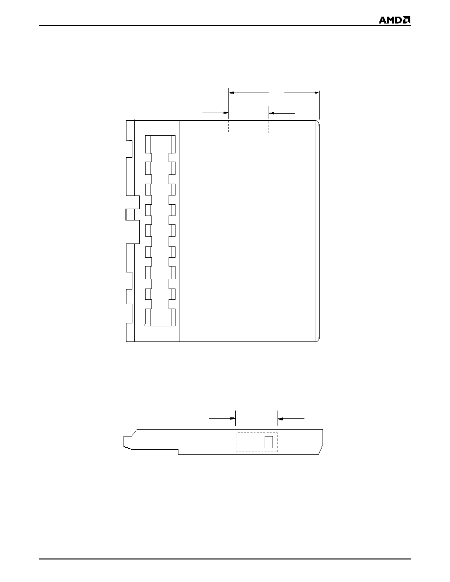
AmMCL00XA 35
P R E L I M I N A R Y
PHYSICAL DIMENSIONS
Bottom View
Right Side View
Write Protect Switch Location
0.245
0.600
Write Protect Switch Location
0.245

36
AmMCL00XA
P R E L I M I N A R Y
REVISION HISTORY FOR AMMCL00XA
Distinctive Characteristics
Added industrial temperature bullet. Revised low
power consumption specifications. Deleted "Small
Form Factor" bullets.
General Description
Revised text to indicate that the Miniature Card specifi-
cation will be defined by PCMCIA. Deleted references
to the elastomeric connector.
Table 2, AMD Flash Miniature Cards and Flash
Devices
Added WP as part of required base part number.
Miniature Card Pad Assignments
BUSY#: Revised to indicate that the Miniature Card
cannot accept most operations when BUSY# is low.
CD#: Deleted last sentence.
Ordering Information
Added Industrial temperature range. Deleted NP option
from part number. Added WP as part of required base
part number.
Figure 2, Host/Card Address Assignments
Labeled host bus in drawing. Deleted NC callouts in
drawing.
Tables 5≠9, Command Definitions
Revised for easier reference: removed "H" designators
from table (now indicated in notes), removed 4-cycle
Reset/Read command, separated Read and Reset
commands, moved RA, RW, RD, PA, PW, PD, X, SA
definitions to legend. Moved Erase Suspend and Erase
Resume definitions from table to notes.
Operating Ranges
Added industrial temperature range.
AC Characteristics, Write Operations
Deleted t
ELQV
, t
AVQV
, t
GLQV
, t
ELQX
, t
EHQZ
, t
GLQX
, t
GHQZ
,
t
AXQX
, t
WHGL
, t
GLQNZ
Embedded Erase Algorithm
Removed last paragraph.
Absolute Maximum Ratings
Revised storage and ambient temperature ratings.
Operating Ranges
Added industrial temperature range.
DC Characteristics
Revised I
CC
specifications. Added frequency specifica-
tion to Note 2.
AC Characteristics, Write (Erase/Program)
Operations
Deleted t
ELQV
, t
AVQV
, t
GLQV
, t
ELQX
, t
EHOZ
, t
GLOX
, t
GHQZ
,
t
AXQ
X, t
WHGL
, t
GLQNZ
.
Table 19, AMD Compatibility Data
Added two tuples of data to list, covering addresses
100h≠10Bh.
Trademarks
Copyright © 1997 Advanced Micro Devices, Inc. All rights reserved.
AMD, the AMD logo, and combinations thereof are trademarks of Advanced Micro Devices, Inc.
Product names used in this publication are for identification purposes only and may be trademarks of their respective companies.