Am29F200A KGD

SUPPLEMENT
1/13/98
Publication# 21257
Rev: B Amendment/0
Issue Date: December 1997
Am29F200A Known Good Die
2 Megabit (256 K x 8-Bit/128 K x 16-Bit)
CMOS 5.0 Volt-only, Sectored Flash Memory--Die Revision 1
DISTINCTIVE CHARACTERISTICS
s
5.0 V
±
10% for read and write operations
-- Minimizes system level power requirements
s
High performance
-- 90 or 120 ns access time
s
Low power consumption
-- 20 mA typical active read current (byte mode)
-- 28 mA typical active read current for
(word mode)
-- 30 mA typical program/erase current
-- 1
µ
A typical standby current
s
Sector erase architecture
-- One 16 Kbyte, two 8 Kbyte, one 32 Kbyte, and
three 64 Kbyte sectors (byte mode)
-- One 8 Kword, two 4 Kword, one 16 Kword, and
three 32 Kword sectors (word mode)
-- Supports full chip erase
-- Sector Protection features:
A hardware method of locking a sector to
prevent any program or erase operations within
that sector
Sectors can be locked via programming
equipment
Temporary Sector Unprotect feature allows code
changes in previously locked sectors
s
Top or bottom boot block configurations
available
s
Embedded Algorithms
-- Embedded Erase algorithm automatically
preprograms and erases the entire chip or any
combination of designated sectors
-- Embedded Program algorithm automatically
writes and verifies data at specified addresses
s
Minimum 100,000 write/erase cycles guaranteed
s
Compatible with JEDEC standards
-- Pinout and software compatible with
single-power-supply flash
-- Superior inadvertent write protection
s
Data# Polling and Toggle Bit
-- Detects program or erase cycle completion
s
Ready/Busy# output (RY/BY#)
-- Hardware method for detection of program or
erase cycle completion
s
Erase Suspend/Resume
-- Supports reading data from a sector not being
erased
s
Hardware RESET# pin
-- Resets internal state machine to the reading
array data
s
Tested to datasheet specifications at
temperature
s
Quality and reliability levels equivalent to
standard packaged components
2
Am29F200A Known Good Die
1/13/98
S U P P L E M E N T
GENERAL DESCRIPTION
The Am29F200A in Known Good Die (KGD) form is a
2 Mbit, 5.0 Volt-only Flash memory. AMD defines KGD
as standard product in die form, tested for functionality
and speed. AMD KGD products have the same reli-
ability and quality as AMD products in packaged form.
Am29F200A Features
The Am29F200A is organized as 262,144 bytes of 8
bits each or 131,072 words of 16 bits each. The 8-bit
data appears on DQ0-DQ7; the 16-bit data appears on
DQ0-DQ15. This device is designed to be programmed
in-system with the standard system 5.0 Volt V
CC
sup-
ply. A 12.0 volt V
PP
is not required for program or erase
operations.
The standard Am29F200A in KGD form offers an ac-
cess time of 90 or 120 ns, allowing high-speed micro-
processors to operate without wait states. To eliminate
bus contention the device has separate chip enable
(CE#), write enable (WE#), and output enable (OE#)
controls.
The device requires only a single 5.0 volt power sup-
ply for both read and write functions. Internally gener-
ated and regulated voltages are provided for the
program and erase operations.
The device is entirely command set compatible with the
JEDEC single-power-supply Flash standard. Com-
mands are written to the command register using stan-
dard microprocessor write timings. Register contents
serve as input to an internal state-machine that con-
trols the erase and programming circuitry. Write cycles
also internally latch addresses and data needed for the
programming and erase operations. Reading data out
of the device is similar to reading from other Flash or
EPROM devices.
Device programming occurs by executing the program
command sequence. This initiates the Embedded
Program algorithm--an internal algorithm that auto-
matically times the program pulse widths and verifies
proper cell margin.
Device erasure occurs by executing the erase com-
mand sequence. This initiates the Embedded Erase
algorithm--an internal algorithm that automatically
preprograms the array ( if it is not already pro-
grammed) before executing the erase operation. Dur-
ing erase, the device automatically times the erase
pulse widths and verifies proper cell margin.
The host system can detect whether a program or
erase operation is complete by observing the RY/BY#
pin, or by reading the DQ7 (Data# Polling) and DQ6/
DQ2 (toggle) status bits. After a program or erase
cycle has been completed, the device is ready to read
array data or accept another command.
The sector erase architecture allows memory sectors
to be erased and reprogrammed without affecting the
data contents of other sectors. The device is fully
erased when shipped from the factory.
Hardware data protection measures include a low
V
CC
detector that automatically inhibits write opera-
tions during power transitions. The hardware sector
protection feature disables both program and erase
operations in any combination of the sectors of mem-
ory. This can be achieved via programming equipment.
The Erase Suspend feature enables the user to put
erase on hold for any period of time to read data from,
or program data to, any sector that is not selected for
erasure. True background erase can thus be achieved.
The hardware RESET# pin terminates any operation
in progress and resets the internal state machine to
reading array data. The RESET# pin may be tied to the
system reset circuitry. A system reset would thus also
reset the device, enabling the system microprocessor
to read the boot-up firmware from the Flash memory.
The system can place the device into the standby mode.
Power consumption is greatly reduced in this mode.
AMD's Flash technology combines years of Flash mem-
ory manufacturing experience to produce the highest lev-
els of quality, reliability and cost effectiveness. The device
electrically erases all bits within a sector simulta-
neously via Fowler-Nordheim tunneling. The data is
programmed using hot electron injection.
ELECTRICAL SPECIFICATIONS
Refer to the Am29F200A data sheet, publication
number 20380, for full electrical specifications on the
Am29F200A.
PRODUCT SELECTOR GUIDE
Family Part Number
Am29F200A KGD
Speed Option (V
CC
= 5.0 V
±
10%)
-90
-120
Max access time, ns (t
ACC
)
90
120
Max CE# access time, ns (t
CE
)
90
120
Max OE# access time, ns (t
OE
)
35
50
1/13/98
Am29F200A Known Good Die
3
S U P P L E M E N T
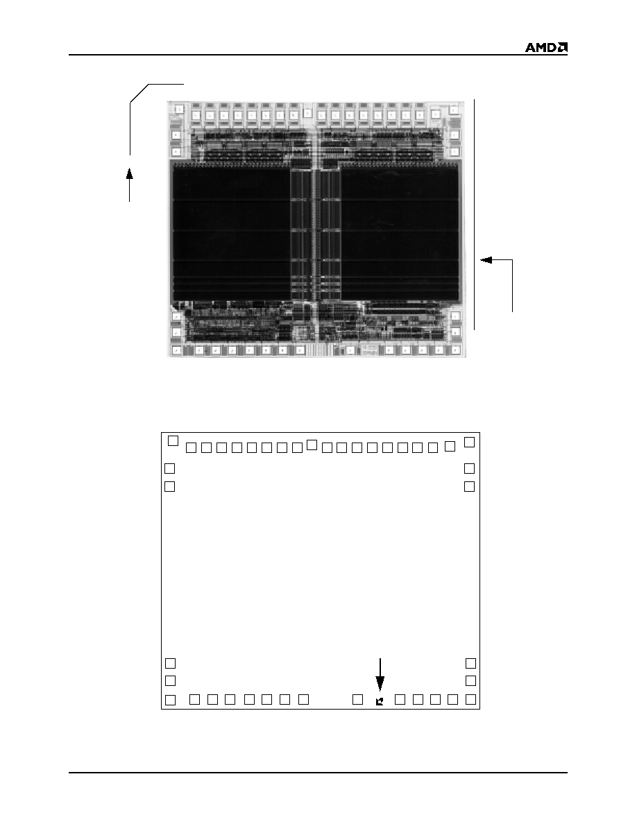
DIE PHOTOGRAPH
DIE PAD LOCATIONS
Orientation relative
to top left corner of
Gel-Pak
Orientation relative
to leading edge of
tape and reel
1
2
3
4
5
6
7
8
9
10
11
12
13
14
15
16 17 18
19 20
21
22
23
24 25
28
29
AMD logo location
30
34
35
36
37
38
39
40
41
31
32
33
26 27
42
4
Am29F200A Known Good Die
1/13/98
S U P P L E M E N T
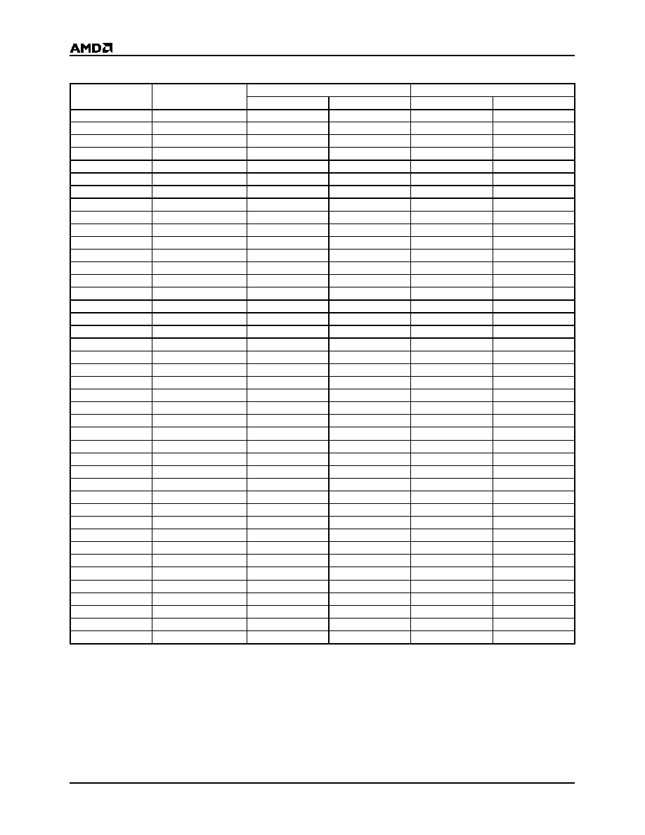
PAD DESCRIPTION
Note: The coordinates above are relative to the center of pad 1 and can be used to operate wire bonding equipment.
Pad
Signal
Pad Center (mils)
Pad Center (millimeters)
X
Y
X
Y
1
V
CC
0.0
0.0
0.0000
0.0000
2
DQ4
8.5
1.2
0.2159
0.0305
3
DQ12
17.3
1.2
0.4394
0.0305
4
DQ5
26.1
1.2
0.6629
0.0305
5
DQ13
34.9
1.2
0.8865
0.0305
6
DQ6
43.6
1.2
1.1074
0.0305
7
DQ14
52.4
1.2
1.3310
0.0305
8
DQ7
61.2
1.2
1.5545
0.0305
9
DQ15/A-1
69.9
1.2
1.7755
0.0305
10
V
SS
80.2
2.7
2.0371
0.0686
11
BYTE#
82.3
13.5
2.0904
0.3429
12
A16
82.3
24.1
2.0904
0.6121
13
A15
82.3
128.4
2.0904
3.2614
14
A14
82.3
138.7
2.0904
3.5230
15
A13
82.3
150.0
2.0904
3.8100
16
A12
68.2
150.0
1.7323
3.8100
17
A11
57.9
150.0
1.4707
3.8100
18
A10
47.6
150.0
1.2090
3.8100
19
A9
36.7
150.0
0.9322
3.8100
20
A8
26.4
150.0
0.6706
3.8100
21
WE#
16.1
150.0
0.4089
3.8100
22
RESET#
5.2
150.0
0.1321
3.8100
23
RY/BY#
26.1
150.0
0.6629
3.8100
24
A7
50.2
150.0
1.2751
3.8100
25
A6
60.5
150.0
1.5367
3.8100
26
A5
70.8
150.0
1.7983
3.8100
27
A4
81.1
150.0
2.0599
3.8100
28
A3
91.4
150.0
2.3216
3.8100
29
A2
91.5
138.7
2.3241
3.5230
30
A1
91.5
128.4
2.3241
3.2614
31
A0
91.5
24.1
2.3241
0.6121
32
CE#
91.5
13.6
2.3241
0.3454
33
V
SS
91.1
1.8
2.3139
0.0457
34
OE#
79.8
0.7
2.0269
0.0178
35
DQ0
70.0
1.2
1.7780
0.0305
36
DQ8
61.3
1.2
1.5570
0.0305
37
DQ1
52.5
1.2
1.3335
0.0305
38
DQ9
43.7
1.2
1.1100
0.0305
39
DQ2
34.9
1.2
0.8865
0.0305
40
DQ10
26.2
1.2
0.6655
0.0305
41
DQ3
17.4
1.2
0.4420
0.0305
42
DQ11
8.6
1.2
0.2184
0.0305
1/13/98
Am29F200A Known Good Die
5
S U P P L E M E N T
ORDERING INFORMATION
Standard Products
AMD standard products are available in several packages and operating ranges. The order number (Valid Combination) is
formed by a combination of the following:
Valid Combinations
Valid Combinations list configurations planned to be sup-
ported in volume for this device. Consult the local AMD sales
office to confirm availability of specific valid combinations and
to check on newly released combinations.
Am29F200A
DEVICE NUMBER/DESCRIPTION
Am29F200A Known Good Die
2 Megabit (256 K x 8-Bit/128 K x 16-Bit) CMOS Flash Memory--Die Revision 1
5.0 Volt-only Read, Program, and Erase
-90
SPEED OPTION
See Valid Combinations
PACKAGE TYPE AND
MINIMUM ORDER QUANTITY
DP =
Waffle Pack
245 die per 5 tray stack
DG =
Gel-Pak
®
Die Tray
486 die per 6 tray stack
DT
=
SurftapeTM (Tape and Reel)
2500 per 7-inch reel
DW = Gel-Pak
®
Wafer Tray (sawn wafer on frame)
Call AMD sales office for minimum order
quantity
TEMPERATURE RANGE
C = Commercial (0
°
C to +70
°
C)
I = Industrial (40
°
C to +85
°
C)
E = Extended (55
°
C to +125
°
C)
DP
C
1
DIE REVISION
This number refers to the specific AMD manufacturing
process and product technology reflected in this
document. It is entered in the revision field of AMD
standard product nomenclature.
T
BOOT CODE SECTOR ARCHITECTURE
T = Top sector
B = Bottom sector
Valid Combinations
Am29F200AT-90,
Am29F200AB-90
DPC 1, DPI 1, DPE 1,
DGC 1, DGI 1, DGE 1,
DTC 1, DTI 1, DTE 1,
DWC 1, DWI 1, DWE 1
Am29F200AT-120,
Am29F200AB-120