 | –≠–ª–µ–∫—Ç—Ä–æ–Ω–Ω—ã–π –∫–æ–º–ø–æ–Ω–µ–Ω—Ç: S2052 | –°–∫–∞—á–∞—Ç—å:  PDF PDF  ZIP ZIP |
1
FIBRE CHANNEL AND GIGABIT ETHERNET TRANSCEIVER
S2052
April 29, 1999 / Revision E
BiCMOS PECL CLOCK GENERATOR
Æ
DEVICE
SPECIFICATION
FIBRE CHANNEL AND GIGABIT ETHERNET TRANSCEIVER
S2052
FEATURES
∑ Functionally compliant with ANSI X3T11 Fibre
Channel physical and transmission protocol
standards and IEEE 802.3Z Gigabit Ethernet
Applications
∑ Transmitter incorporates phase-locked loop
(PLL) providing clock synthesis from low-speed
reference
∑ Receiver PLL configured for clock and data
recovery
∑ 1250 and 1062 Mb/s operation
∑ 10-bit parallel TTL compatible interface
∑ 800mW typical power dissipation
∑ +3.3V power supply
∑ Low-jitter serial PECL compatible interface
∑ Lock detect
∑ Local loopback
∑ 64 PQFP package
∑ Fibre Channel framing performed by receiver
∑ Continuous downstream clocking from receiver
∑ Drives 30m of Twinax cable directly
APPLICATIONS
High-speed data communications
∑ Workstation
∑ Frame buffer
∑ Switched networks
∑ Data broadcast environments
∑ Proprietary extended backplanes
∑ RAID drives
∑ Mass storage devices
GENERAL DESCRIPTION
The S2052 transmitter and receiver chip is designed
to perform high-speed serial data transmission over
fiber optic or coaxial cable interfaces conforming to
the requirements of the ANSI X3T11 Fibre Channel
specification. The chip runs at 1250.0, and 1062.5
Mbit/s data rates with associated 10-bit data word.
The chip performs parallel-to-serial and serial-to-par-
allel conversion and framing for block-encoded data.
The transmitter's on-chip PLL synthesizes the high-
speed clock from a low-speed reference. The
receiver's on-chip PLL synchronizes directly to incom-
ing digital signal to receive the data stream. The
transmitter and receiver each support differential
PECL-compatible I/O for fiber optic component inter-
faces, to minimize crosstalk and maximize data
integrity. Local loopback mode is provided for system
diagnostics.
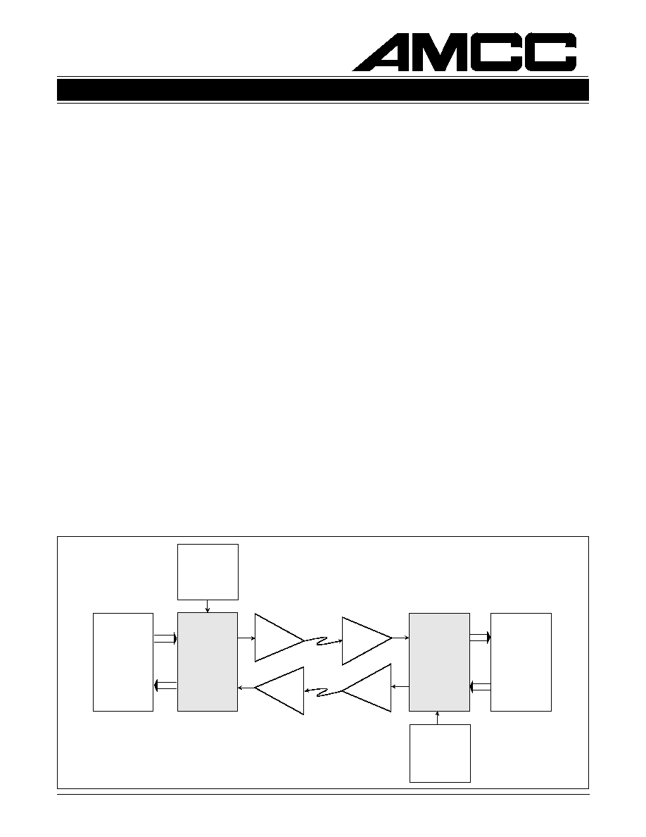
Figure 1 shows a typical configuration incorporating
the chip, which is compatible with AMCC's S2036
Open Fiber Control (OFC) device.
Figure 1. System Block Diagram
Optical
TX
Optical
RX
Optical
RX
Optical
TX
S2036
Open
Fiber
Control
(OFC)
S2036
Open
Fiber
Control
(OFC)
S2052
S2052
Gigabit
Ethernet
Controller
Gigabit
Ethernet
Controller
2
FIBRE CHANNEL AND GIGABIT ETHERNET TRANSCEIVER
S2052
April 29, 1999 / Revision E
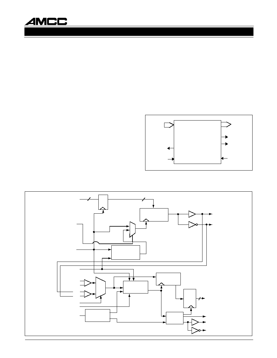
Internal clocking and control functions are transpar-
ent to the user. Details of data timing can be seen in
Figure 4. A block diagram showing the basic chip
operation is shown in Figure 3.
Loopback
Local loopback is supported by the chip, and pro-
vides a capability for performing offline testing of the
interface to ensure the integrity of the serial channel
before enabling the transmission medium. It also al-
lows for system diagnostics.
S2052 OVERVIEW
The S2052 transmitter and receiver provide serializa-
tion and deserialization functions for block-encoded
data to implement a Fibre Channel interface. Opera-
tion of the S2052 is straightforward, as depicted in
Figure 2. The sequence of operations is as follows:
Transmitter
1. 10-bit parallel input
2. Parallel-to-serial conversion
3. Serial output
Receiver
1. Clock and data recovery from serial input
2. Serial-to-parallel conversion
3. Frame detection
4. 10-bit parallel output
The 10-bit parallel data handled by the S2052 device
should be from a DC-balanced encoding scheme, such
as the 8B/10B transmission code, in which informa-
tion to be transmitted is encoded 8 bits at a time into
10-bit transmission characters
1
, and be compliant with
ANSI X3.230 FC-PH (Fibre Channel Physical and Sig-
naling Interface).
Figure 2. Interface Diagram
Parallel
Data In
S2052
Transceiver
TBC
Serial
Data In
RBC
Parallel
Data Out
COM_DET
Serial
Data Out
TXTESTN
TX [0:9]
10
10
PLL CLOCK
MULTIPLIER
F0 = F1 X 10
SHIFT
REGISTER
TXP
TXN
D
Q
PLL CLOCK
RECOVERY
2:1
D
10
D
BITCLK
Q
COM_DET
DETECT
LOGIC
CONTROL
LOGIC
RXP
TBC
RXBYPN
RXN
TP
TN
EWRAP
-LCK_REF
EN_CDET
RX[0:9]
RBC1
COM_DET
RBC0
SHIFT
REGISTER
Input
Latch
Figure 3. Functional Block Diagram
3
FIBRE CHANNEL AND GIGABIT ETHERNET TRANSCEIVER
S2052
April 29, 1999 / Revision E
TBC
(Input)
RBC0
(Output)
COM_DET
(Output)
PARALLEL
DATA BUS
(Input)
PARALLEL
DATA BUS
(Output)
SERIAL DATA
K28.5
Byte 1
Byte 2
Byte 3
Byte 4
Byte 5
K28.5
K28.5
K28.5
K28.5
K28.5
RBC1
(Output)
1. A.X. Widmer and P.A. Franaszek, "A Byte-Oriented DC Balanced (0,4) 8B/10B Transmission Code," IBM Research Report RC 9391,
May 1982.
Figure 4. Functional Waveform (1250 and 1062.5 Mbit/sec)
Data Byte
9
8
7
6
5
4
3
2
1
0
TX[0:9] or
RX[0:9]
8b/10b alphabetic
representation
j
h
g
f
i
e
d
c
b
a
Table 1. Data Mapping to 8b/10b
Alphabetic Representation
TRANSMITTER FUNCTIONAL
DESCRIPTION
The S2052 transmitter accepts parallel input data and
serializes it for transmission over fiber optic or coaxial
cable media. The chip is fully compatible with the ANSI
X3T11 Fibre Channel standard, and supports the Fi-
bre Channel Gigabit Ethernet standard's data rates of
1250 and 1062 Mbit/sec. (See Figure 3.)
Parallel/Serial Conversion
The parallel-to-serial converter takes in 10-bit wide
data from the input latch and converts it to a serial
data stream. Parallel data is latched into the transmitter
on the positive going edge of TBC. The data is then
clocked synchronous to the clock synthesis unit serial
clock into the serial output shift register. The shift
register is clocked by the internally generated bit clock
which is 10x of the TBC inputfrequency. D0 is trans-
mitted first as described in annex N and Tables 22
and 23 of FC-PH. Table 1 shows the mapping of the
parallel data to the 8B/10B codes.
Transmit Byte Clock
The transmit byte clock input (TBC) must be supplied
with a clock source with 100 PPM tolerance to assure
that the transmitted data meets the Fibre Channel fre-
quency limits. The internal serial clock is frequency locked
to the reference clock (125.00 and 106.25 MHz).
RECEIVER FUNCTIONAL DESCRIPTION
The S2052 receiver is designed to implement the ANSI
X3T11 Fibre Channel specification and the IEEE 802.3Z
Gigabit Ethernet receiver functions. A block diagram
showing the basic chip function is provided in Figure 3.
Whenever a signal is present, the S2052 attempts to
achieve synchronization on both bit and transmission-
word boundaries of the received encoded bit stream.
Received data from the incoming bit stream is pro-
vided on the device's parallel data outputs.
The S2052 accepts serial encoded data from a fiber
optic or coaxial cable interface. The serial input stream is
the result of the serialization of 8B/10B encoded data by
an FC compatible transmitter. Clock recovery is performed
on-chip, with the output data presented to the Fibre
Channel transmission layer as 10-bit parallel data.

4
FIBRE CHANNEL AND GIGABIT ETHERNET TRANSCEIVER
S2052
April 29, 1999 / Revision E
Serial/Parallel Conversion
Serial data is received on the RX, RY pins. The PLL
clock recovery circuit will lock to the data stream if
the clock to be recovered is within
±
100 PPM of the
internally generated bit rate clock. The recovered clock
is used to retime the input data stream. The data is
then clocked into the serial to parallel output regis-
ters. Data is clocked out on the rising edge of RBC1
and RBC0. The parallel data out is 10 bits wide. The
word clock (RBC1) is synchronized to the incoming
data stream word boundary by the detection of the
Fibre Channel Comma character, positive disparity
(0011111XXXX), found in the K28.5 control character.
Transmit Byte Clock Input
The transmit byte clock input must be supplied with a
TTL clock source at
±
100 PPM tolerance.
Framing
The S2052 provides COM_DET character recognition
and data word alignment of the TTL compatible output
data bus. In systems where the COM_DET function is
undesired, a LOW on the EN_CDET input disables the
COM_DET function and the data will be "un-framed".
When framing is disabled by low EN_CDET, the S2052
simply achieves bit synchronization within 250 bit times
and begins to deliver parallel output data words when-
ever it has received full transmission words. No attempt
is made to synchronize on any particular incoming char-
acter.
The COM_DET output signal will go high whenever a
positive disparity comma character, found in the K28.5
control character, is present on the parallel data out-
puts. The COM_DET output signal will be low at all
other times.
Lock Detect
The S2052 lock detect function monitors the state of
the receiver phase-locked loop (PLL) clock recovery
unit. The PLL will lock within 250 bit times after the
start of receiving serial data inputs. If the serial data
inputs have an instantaneous phase jump (from a se-
rial switch, for example) the PLL will not indicate an
out-of-lock state, but will recover the correct phase align-
ment within 50 to 250 bit times, depending on the input
eye opening. (See Fig. 14). If a run length of 80-160
bits is exceeded, or if the input data rate varies by
more than 1000 ppm compared to the reference clock,
the loop will be declared out of lock. When lock is lost,
the PLL will shift from the serial input data to the refer-
ence clock, so that the downstream clock will maintain
the correct frequency.
In any transfer of PLL control from the serial data to the
reference clock, the RBC1/RBC0 output remains phase
continuous and glitch free, assuring the integrity of down-
stream clocking.
OTHER OPERATING MODES
Loopback
When local loopback is enabled, serial data from the
transmitter is internally routed to the receiver, where
the clock is extracted and the data is deserialized. The
parallel data is then sent to the subsystem for verifica-
tion. This loopback mode provides the capability to
perform offline testing of the interface to guarantee the
integrity of the serial channel before enabling the trans-
mission medium. It also allows system diagnostics.
Operating Frequency Range
The S2052 is optimized for operation at 1250 and
1062 Mbit/s. Operation at other rates is possible if the
rate falls between the nominal rates. REFCLK must
be selected to be within 100 ppm of the desired byte
or word clock rate.

5
FIBRE CHANNEL AND GIGABIT ETHERNET TRANSCEIVER
S2052
April 29, 1999 / Revision E
S2052 Transmitter Pin Assignment and Descriptions
e
m
a
N
n
i
P
l
e
v
e
L
O
/
I
#
n
i
P
n
o
i
t
p
i
r
c
s
e
D
9
X
T
8
X
T
7
X
T
6
X
T
5
X
T
4
X
T
3
X
T
2
X
T
1
X
T
0
X
T
L
T
T
I
3
1
2
1
1
1
9
8
7
6
4
3
2
e
h
t
n
o
n
i
d
e
k
c
o
l
c
s
i
s
u
b
s
i
h
t
n
o
a
t
a
d
l
e
ll
a
r
a
P
.
a
t
a
d
t
i
m
s
n
a
r
T
.
t
s
r
i
f
d
e
t
t
i
m
s
n
a
r
t
s
i
0
X
T
.
C
B
T
f
o
e
g
d
e
g
n
i
s
i
r
C
B
T
L
T
T
I
2
2
d
e
ll
o
r
t
n
o
c
-
l
a
t
s
y
r
c
a
,
k
c
o
l
c
e
t
y
b
t
i
m
s
n
a
r
t
d
n
a
k
c
o
l
c
e
c
n
e
r
e
f
e
R
f
o
y
c
n
e
u
q
e
r
f
e
h
T
.
r
e
il
p
i
t
l
u
m
k
c
o
l
c
L
L
P
e
h
t
r
o
f
k
c
o
l
c
e
c
n
e
r
e
f
e
r
.
0
1
y
b
d
e
d
i
v
i
d
e
t
a
r
t
i
b
e
h
t
s
i
C
B
T
N
T
S
E
T
X
T
L
T
T
I
0
1
e
t
a
t
il
i
c
a
f
o
t
k
c
o
l
c
t
i
b
X
T
l
a
n
r
e
t
n
i
s
e
c
a
l
p
e
r
C
B
T
,
W
O
L
n
e
h
W
C
B
T
e
h
t
o
t
k
c
o
l
ll
i
w
L
L
P
X
T
e
h
t
,
H
G
I
H
n
e
h
W
.
g
n
i
t
s
e
t
y
r
o
t
c
a
f
.
t
u
p
n
i
P
X
T
N
X
T
.
f
f
i
D
L
C
E
P
O
2
6
1
6
r
e
t
t
i
m
s
n
a
r
t
l
a
i
r
e
s
e
h
t
t
u
o
d
n
e
s
t
a
h
t
s
t
u
p
t
u
o
L
C
E
P
l
a
i
t
n
e
r
e
f
f
i
D
5
7
e
v
i
r
d
d
n
a
a
t
a
d
0
5
r
o
e
h
t
s
i
P
X
T
.
V
2
≠
c
c
V
o
t
n
o
i
t
a
n
i
m
r
e
t
.
t
u
p
t
u
o
e
v
i
t
a
g
e
n
e
h
t
s
i
N
X
T
d
n
a
,
t
u
p
t
u
o
e
v
i
t
i
s
o
p