 | ÐлекÑÑоннÑй компоненÑ: AS7C3513A | СкаÑаÑÑ:  PDF PDF  ZIP ZIP |
AS7C3513Av.0.9.3.fm
September 2001
Preliminary Information
&RS\ULJKW $OOLDQFH 6HPLFRQGXFWRU $OO ULJKWV UHVHUYHG
AS7C513A
AS7C3513A
5V/3.3V 32K×16 CMOS SRAM
Y
$OOLDQFH 6HPLFRQGXFWRU
3 RI
)HDWXUHV
· AS7C513A (5V version)
· AS7C3513A (3.3V version)
· Industrial and commercial temperature
· Organization: 32,768 words × 16 bits
· Center power and ground pins
· High speed
- 10/12/15/20 ns address access time
- 5, 6, 7, 8 ns output enable access time
· Low power consumption: ACTIVE
- 660 mW (AS7C513) / max @ 10 ns
- 324 mW (AS7C3513) / max @ 10 ns
· Low power consumption: STANDBY
- 55 mW (AS7C513A) / max CMOS
- 36 mW (AS7C3513A) / max CMOS
· Latest 6T 0.25 CMOS Technology
· Easy memory expansion with CE, OE inputs
· TTL-compatible, three-state I/O
· 44-pin JEDEC standard package
- 400 mil SOJ
- 400 mil TSOP 2
· ESD protection
2000 volts
· Latch-up current
200 mA
µ
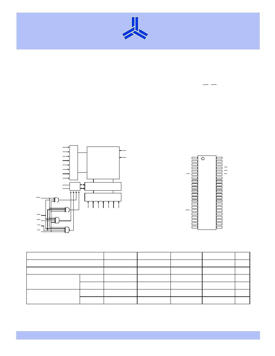
/RJLF EORFN GLDJUDP
32K × 16
Array
OE
CE
WE
Column decoder
R
o
w d
e
coder
A0
A1
A2
A3
A4
A5
A7
V
CC
GND
A8
A9
A10
A11
A12
A13
A14
Control circuit
I/O0I/O7
I/O8I/O15
UB
LB
I/O
buffer
A6
3LQ DUUDQJHPHQW
5
6
7
8
9
10
11
12
13
14
15
16
17
18
19
20
I/O13
I/O12
GND
V
CC
I/O11
I/O10
I/O9
I/O8
NC
A7
A8
A9
A10
NC
A0
CE
I/O0
I/O1
I/O2
I/O3
V
CC
GND
I/O4
I/O5
I/O6
I/O7
WE
A14
A13
A12
44-Pin SOJ, TSOP 2 (400 mil)
21
22
A11
NC
UB
LB
I/O15
I/O14
2
A3
3
A2
4
A1
1
NC
40
39
38
37
36
35
34
33
32
31
30
29
28
27
26
25
24
23
43
42
41
44
A5
A6
OE
A4
A
S
7C513A
A
S
7C3513A
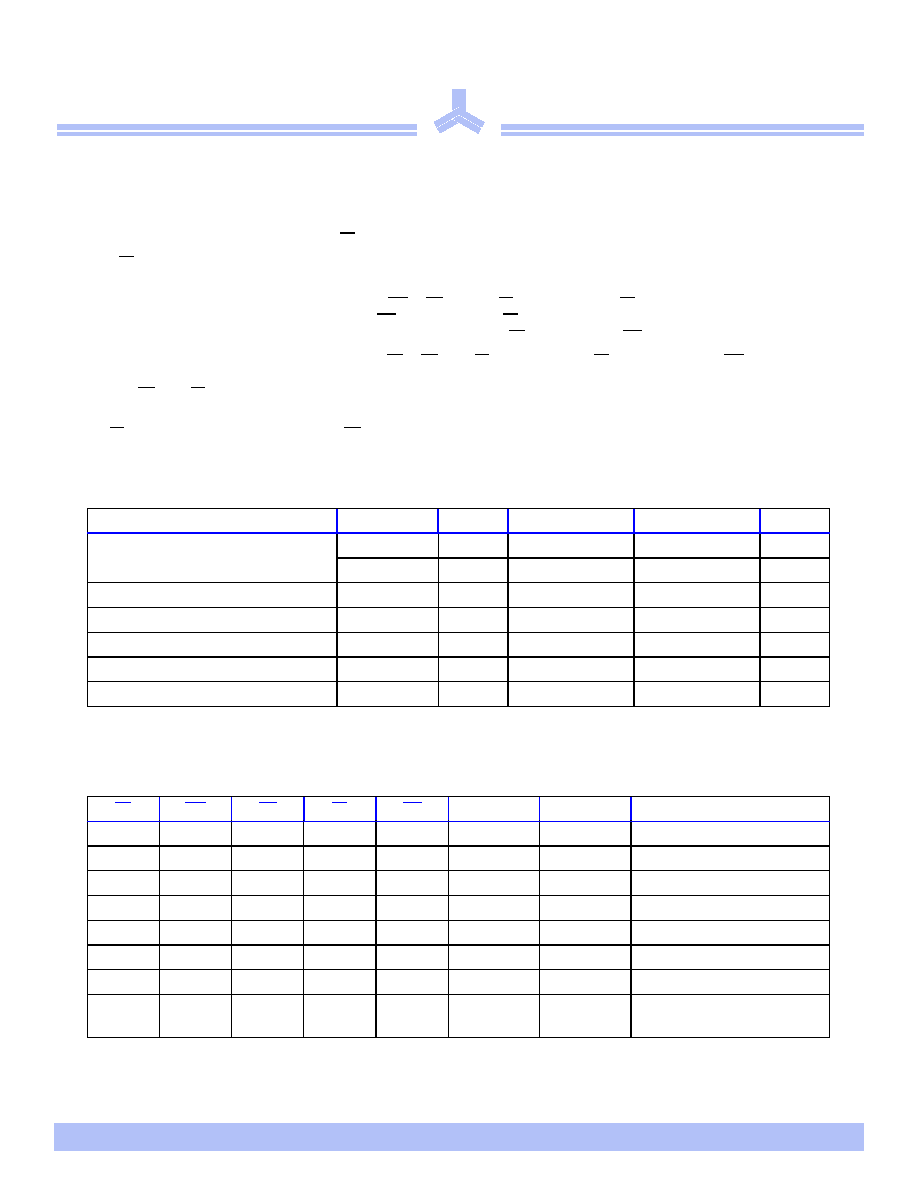
6HOHFWLRQ JXLGH
-10
-12
-15
-20
Unit
Maximum address access time
10
12
15
20
ns
Maximum output enable access time
5
6
7
8
ns
Maximum operating current
AS7C513A
120
110
100
100
mA
AS7C3513A
90
80
80
80
mA
Maximum CMOS standby
current
AS7C513A
10
10
10
15
mA
AS7C3513A
10
10
10
15
mA
$6&$
$6&$
Y
$OOLDQFH 6HPLFRQGXFWRU
3 RI
)XQFWLRQDO GHVFULSWLRQ
The AS7C513A and the AS7C3513A are high performance CMOS 524,288-bit Static Random Access Memory (SRAM) devices organized as
32,768 words × 16 bits. They are designed for memory applications where fast data access, low power, and simple interfacing are desired.
Equal address access and cycle times (t
AA
, t
RC
, t
WC
) of 10/12/15/20 ns with output enable access times (t
OE
) of 5, 6, 7, 8 ns are ideal for high
performance applications. The chip enable input CE permits easy memory expansion with multiple-bank memory systems.
When CE is high, the devices enter standby mode. The AS7C513A and AS7C3513A are guaranteed not to exceed 55/36 mW power
consumption in CMOS standby mode.
A write cycle is accomplished by asserting write enable (WE), (UB) and/or (LB), and chip enable (CE). Data on the input pins I/O0-I/O7,
and/or I/O8I/O15, is written on the rising edge of WE (write cycle 1) or CE (write cycle 2). To avoid bus contention, external devices
should drive I/O pins only after outputs have been disabled with output enable (OE) or write enable (WE).
A read cycle is accomplished by asserting output enable (OE), (UB) and (LB), and chip enable (CE), with write enable (WE) high. The chips
drive I/O pins with the data word referenced by the input address. When either chip enable or output enable is inactive, or write enable is
active, or (UB) and (LB), output drivers stay in high-impedance mode.
The devices provide multiple center power and ground pins, and separate byte enable controls, allowing individual bytes to be written and
read. LB controls the lower bits, I/O0I/O7, and UB controls the higher bits, I/O8I/O15.
All chip inputs and outputs are TTL-compatible. The AS7C513A and AS7C3513A are packaged in common industry standard packages.
$EVROXWH PD[LPXP UDWLQJV
NOTE: Stresses greater than those listed under Absolute Maximum Ratings may cause permanent damage to the device. This is a stress rating only and functional oper-
ation of the device at these or any other conditions outside those indicated in the operational sections of this specification is not implied. Exposure to absolute
maximum rating conditions for extended periods may affect reliability.
7UXWK WDEOH
Key: X = Don't care; L = Low; H = High
Parameter
Device
Symbol
Min
Max
Unit
Voltage on V
CC
relative to GND
AS7C513A
V
t1
0.50
+7.0
V
AS7C3513A
V
t1
0.50
+5.0
V
Voltage on any pin relative to GND
V
t2
0.50
V
CC
+0.50
V
Power dissipation
P
D
1.0
W
Storage temperature (plastic)
T
stg
65
+150
o
C
Ambient temperature with V
CC
applied
T
bias
55 +125
o
C
DC current into outputs (low)
I
OUT
50
mA
CE
WE
OE
LB
UB
I/O0I/O7
I/O8I/O15
Mode
H
X
X
X
X
High Z
High Z
Standby (I
SB
, I
SBI
)
L
H
L
L
H
D
OUT
High Z
Read I/O0I/O7 (I
CC
)
L
H
L
H
L
High Z
D
OUT
Read I/O8I/O15 (I
CC
)
L
H
L
L
L
D
OUT
D
OUT
Read I/O0I/O15 (I
CC
)
L
L
X
L
L
D
IN
D
IN
Write I/O0I/O15 (I
CC
)
L
L
X
L
H
D
IN
High Z
Write I/O0I/O7 (I
CC
)
L
L
X
H
L
High Z
D
IN
Write I/O8I/O15 (I
CC
)
L
L
H
X
H
X
X
H
X
H
High Z
High Z
Output disable (I
CC
)
$6&$
$6&$
Y
$OOLDQFH 6HPLFRQGXFWRU
3 RI
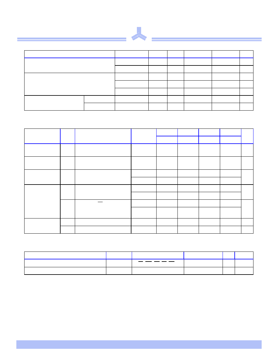
5HFRPPHQGHG RSHUDWLQJ FRQGLWLRQV
V
IL
min = 3.0V for pulse width less than t
RC
/2.
'& RSHUDWLQJ FKDUDFWHULVWLFV RYHU WKH RSHUDWLQJ UDQJH�
&DSDFLWDQFH I 0+] 7
D
R
& 9
&&
120,1$/�
Parameter
Device
Symbol
Min
Typical
Max
Unit
Supply voltage
AS7C513A
V
CC
4.5
5.0
5.5
V
AS7C3513A
V
CC
3.0
3.3
3.6
V
Input voltage
AS7C513A
V
IH
2.2
V
CC
+ 0.5
V
AS7C3513A
V
IH
2.0
V
CC
+ 0.5
V
IL
0.5
0.8
V
Ambient operating temperature
commercial
T
A
0
70
° C
industrial
T
A
40
05
° C
Parameter
Sym
Test conditions
Device
-10
-12
-15
-20
Unit
Min Max Min Max Min Max Min Max
Input leakage
current
|
I
LI
|
V
CC
= Max
V
IN
= GND to V
CC
1
1
1
1
µA
Output leakage
current
|
I
LO
|
V
CC
= Max
V
OUT
= GND to V
CC
1
1
1
1
µA
Operating power
supply current
I
CC
V
CC
= Max, CE
V
IL
f = f
Max
, I
OUT
= 0mA
AS7C513A
120
110
100
100
mA
AS7C3513A
90
80
80
80
Standby power
supply current
I
SB
V
CC
= Max, CE
V
IL
f = f
Max
, I
OUT
= 0mA
AS7C513A
30
25
20
20
mA
AS7C3513A
30
25
20
20
I
SB1
V
CC
=
Max, CE
V
CC
0.2V
V
IN
GND + 0.2V or
CMOS V
IN
V
CC
0.2V, f = 0
AS7C513A
10
10
10
15
mA
AS7C3513A
10
10
10
15
Output voltage
V
OL
I
OL
= 8 mA, V
CC
= Min
0.4
0.4
0.4
0.4
V
V
OH
I
OH
= 4 mA, V
CC
= Min
2.4
2.4
2.4
2.4
V
Parameter
Symbol
Signals
Test conditions
Max
Unit
Input capacitance
C
IN
A, CE, WE, OE, LB, UB
V
in
= 0V
5
pF
I/O capacitance
C
I/O
I/O
V
in
= V
out
= 0V
7
pF
$6&$
$6&$
Y
$OOLDQFH 6HPLFRQGXFWRU
3 RI
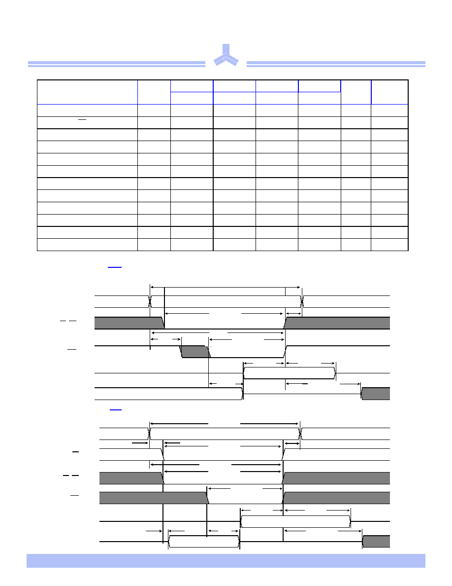
5HDG F\FOH RYHU WKH RSHUDWLQJ UDQJH�
.H\ WR VZLWFKLQJ ZDYHIRUPV
5HDG ZDYHIRUP DGGUHVV FRQWUROOHG�
5HDG ZDYHIRUP &( 2( 8% /% FRQWUROOHG�
Parameter
Symbol
-10
-12
-15
-20
Unit
Notes
Min
Max
Min
Max
Min
Max
Min
Max
Read cycle time
t
RC
10
12
15
20
ns
Address access time
t
AA
10
12
15
20
ns
3
Chip enable (CE) access time
t
ACE
10
12
15
20
ns
3
Output enable (OE) access time
t
OE
5
6
7
8
ns
Output hold from address change t
OH
2
3
3
3
ns
5
CE Low to output in low Z
t
CLZ
0
0
0
0
ns
4, 5
CE High to output in high Z
t
CHZ
3
6
4
5
ns
4, 5
OE Low to output in low Z
t
OLZ
0
0
0
0
ns
4, 5
Byte select access time
t
BA
5
6
7
8
ns
Byte select Low to low Z
t
BLZ
0
0
0
0
ns
4,5
Byte select High to high Z
t
BHZ
5
6
6
8
ns
4,5
OE High to output in high Z
t
OHZ
3
4
4
5
ns
4, 5
Power up time
t
PU
0
0
0
0
ns
4, 5
Power down time
t
PD
10
12
15
20
ns
4, 5
Undefined output/don't care
Falling input
Rising input
t
OH
t
AA
t
RC
t
OH
Data OUT
Address
Data valid
Previous data valid
Data valid
t
RC
t
AA
t
BLZ
t
BA
t
OE
t
OLZ
t
OH
t
OHZ
t
HZ
t
BHZ
t
ACE
t
LZ
Address
OE
CE
LB, UB
Data OUT
$6&$
$6&$
Y
$OOLDQFH 6HPLFRQGXFWRU
3 RI
:ULWH F\FOH RYHU WKH RSHUDWLQJ UDQJH�
:ULWH ZDYHIRUP :( FRQWUROOHG�
:ULWH ZDYHIRUP &( FRQWUROOHG�
Parameter
Symbol
-10
-12
-15
-20
Unit
Notes
Min
Max
Min
Max
Min
Max
Min
Max
Write cycle time
t
WC
10
12
15
20
ns
Chip enable (CE) to write end
t
CW
8
10
12
12
ns
Address setup to write end
t
AW
8
9
10
12
ns
Address setup time
t
AS
0
0
0
0
ns
Write pulse width
t
WP
7
8
9
12
ns
Write recovery time
t
WR
0
0
0
0
ns
Address hold from end of write
t
AH
0
0
0
0
ns
Data valid to write end
t
DW
5
6
8
10
ns
Data hold time
t
DH
0
0
0
0
ns
5
Write enable to output in high Z t
WZ
6
6
6
8
ns
4, 5
Output active from write end
t
OW
1
1
1
2
ns
4, 5
Byte select Low to end of write
t
BW
8
10
12
12
ns
Address
LB, UB
WE
Data IN
Data OUT
t
WC
t
BW
t
AW
t
AS
t
WP
t
DW
t
DH
t
OW
t
WZ
Data undefined
High-Z
Data valid
t
WR
Address
CE
LB, UB
WE
Data IN
t
WC
t
CW
t
BW
t
WP
t
DW
t
DH
t
OW
t
WZ
t
AH
Data OUT
Data undefined
High-Z
High-Z
t
AS
t
AW
Data valid
t
CLZ
t
WR
&