AS7C33512PFS32_36.V032003.fm
March 2003
Advance Information
Copyright © Alliance Semiconductor. All rights reserved.
®
AS7C33512PFS32A
AS7C33512PFS36A
4/8/03, v. 032003 Advance Info
Alliance Semiconductor
1 of 21
3.3V 512K
×
32/36 pipelined burst synchronous SRAM
Features
· Organization: 524,288 words × 32 or 36 bits
· Fast clock speeds to 200MHz in LVTTL/LVCMOS
· Fast clock to data access:
3/3.4/3.8 ns
· Fast OE access time: 3/3.4/3.8 ns
· Fully synchronous register-to-register operation
· Single register flow-through mode
· Single-cycle deselect
- Dual-cycle deselect also available (AS7C331MPFD18A,
AS7C33512PFD32A/ AS7C33512PFD36A)
· Asynchronous output enable control
· Available in 100-pin TQFP package and 165-ball BGA
· Individual byte write and global write
· Multiple chip enables for easy expansion
· 3.3V core power supply
· 2.5V or 3.3V I/O operation with separate V
DDQ
· Linear or interleaved burst control
· Snooze mode for reduced power-standby
· Common data inputs and data outputs
· Boundary scan using IEEE 1149.1 JTAG function
· NTDTM
1
pipelined architecture available
(AS7C331MNTD18A, AS7C33512NTD32A/
AS7C33512NTD36A)
1 NTDTM is a trademark of Alliance Semiconductor Corporation. All trademarks
mentioned in this document are the property of their respective owners.
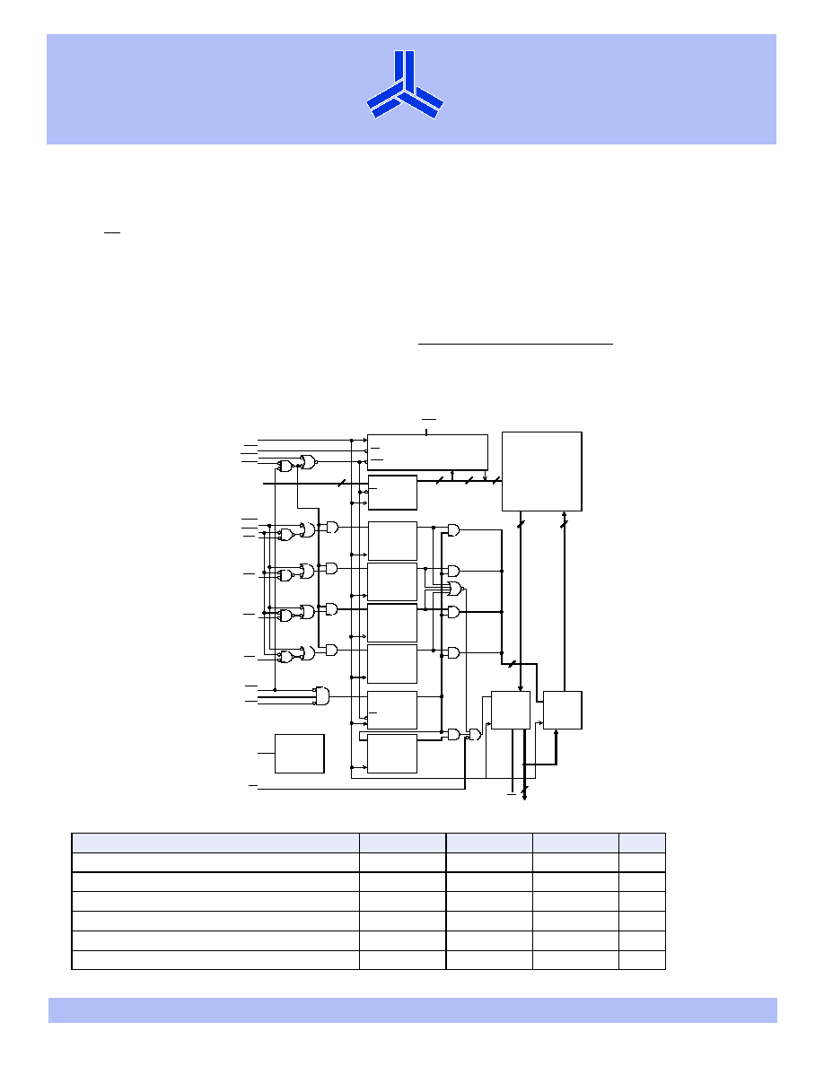
Logic block diagram
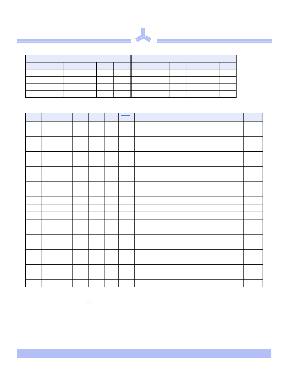
Selection guide
-200
-166
-133
Units
Minimum cycle time
5
6
7.5
ns
Maximum clock frequency
200
166
133
MHz
Maximum pipelined clock access time
3.0
3.4
3.8
ns
Maximum operating current
400
350
325
mA
Maximum standby current
130
120
110
mA
Maximum CMOS standby current (DC)
70
70
70
mA
Q0
Q1
512K × 32/36
Memory
array
Burst logic
CLK
CLR
CE
Address
D
Q
CE
CLK
DQ
d
CLK
D
Q
Byte write
registers
register
DQ
c
CLK
D
Q
Byte write
registers
DQ
b
CLK
D
Q
Byte write
registers
DQ
a
CLK
D
Q
Byte write
registers
Enable
CLK
D
Q
register
Enable
CLK
D
Q
delay
register
CE
Output
registers
Input
registers
Power
down
DQ[a:d]
4
36/32
19
17
19
19
GWE
BWE
BW
d
ADV
ADSC
ADSP
CLK
CE0
CE1
CE2
BW
c
BW
b
BW
a
OE
ZZ
LBO
OE
FT
CLK
CLK
36/32
36/32
A[18:0]
4/8/03, v. 032003 Advance Info
Alliance Semiconductor
2 of 21
AS7C33512PFS32A
AS7C33512PFS36A
®
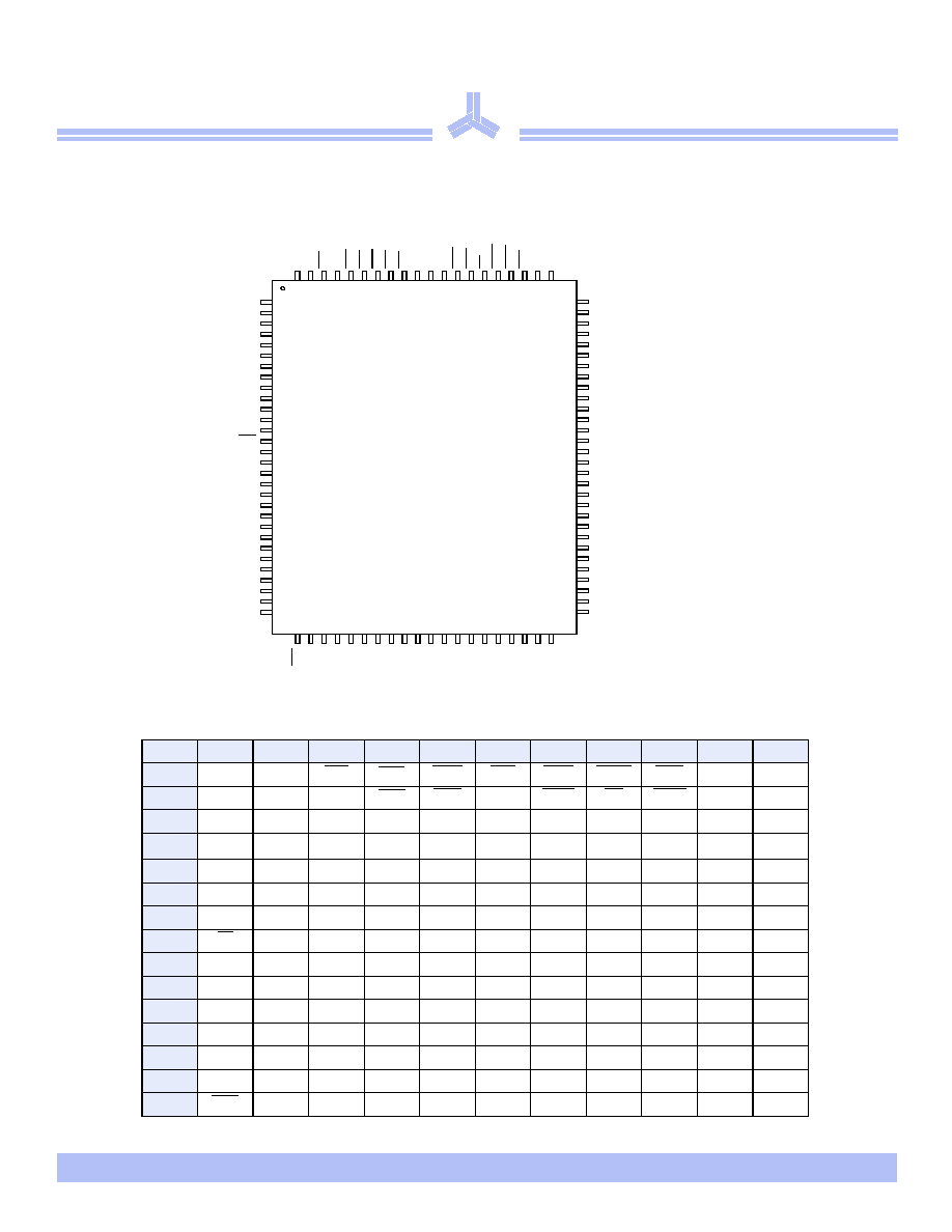
Pin and ball assignment
100-pin TQFP - top view
Ball assignment for 165-ball BGA for 512K x 36
1
2
3
4
5
6
7
8
9
10
11
A
NC
A
CE0
BWc
BWb
CE2
BWE
ADSC
ADV
A
NC
B
NC
A
CE1
BWd
BWa
CLK
GWE
OE
ADSP
A
NC
C
DQPc
NC
V
DDQ
V
SS
V
SS
V
SS
V
SS
V
SS
V
DDQ
NC
DQPb
D
DQc
DQc
V
DDQ
V
DD
V
SS
V
SS
V
SS
V
DD
V
DDQ
DQb
DQb
E
DQc
DQc
V
DDQ
V
DD
V
SS
V
SS
V
SS
V
DD
V
DDQ
DQb
DQb
F
DQc
DQc
V
DDQ
V
DD
V
SS
V
SS
V
SS
V
DD
V
DDQ
DQb
DQb
G
DQc
DQc
V
DDQ
V
DD
V
SS
V
SS
V
SS
V
DD
V
DDQ
DQb
DQb
H
FT
NC
NC
V
DD
V
SS
V
SS
V
SS
V
DD
NC
NC
ZZ
J
DQd
DQd
V
DDQ
V
DD
Vss
V
SS
V
SS
V
DD
V
DDQ
DQa
DQa
K
DQd
DQd
V
DDQ
V
DD
Vss
V
SS
V
SS
V
DD
V
DDQ
DQa
DQa
L
DQd
DQd
V
DDQ
V
DD
Vss
V
SS
V
SS
V
DD
V
DDQ
DQa
DQa
M
DQd
DQd
V
DDQ
V
DD
Vss
V
SS
V
SS
V
DD
V
DDQ
DQa
DQa
N
DQPd
NC
V
DDQ
V
SS
NC
A
NC
V
SS
V
DDQ
NC
DQPa
P
NC
NC
A
A
TDI
A1
1
1 A0 and A1 are the two least significant bits (LSB) of the address field and set the internal burst counter if burst is desired.
TDO
A
A
A
A
R
LBO
NC
A
A
TMS
A0
1
TCK
A
A
A
A
/%2
$ $ $ $ $ $ 1& 1& 9
66
9
''
$ $ $ $ $ $ $ $
$ $
&(
&(
%:G %:F %:E %:
D
&(
9
''
9
66
&/. *:( %:( 2( $'
6&
$'
63
$'
9
$ $
74)3 [ PP
$
1&'43F
'4F
'4F
9
''4
9
664
'4F
'4F
'4F
'4F
9
664
9
''4
'4F
'4F
)7
9
''
1&
9
66
'4G
'4G
9
''4
9
664
'4G
'4G
'4G
'4G
9
664
9
''4
'4G
'4G
1&'43G
'43E1&
'4E
'4E
9
''4
9
664
'4E
'4E
'4E
'4E
9
664
9
''4
'4E
'4E
9
66
==
'4D
'4D
9
''4
9
664
'4D
'4D
'4D
'4D
9
664
9
''4
'4D
'4D
'43D1&
9
''
1&
1RWH )RU SLQV DQG 1& DSSOLHV WR WKH [ FRQILJXUDWLRQ '43Q DSSOLHV WR WKH [
4/8/03, v. 032003 Advance Info
Alliance Semiconductor
3 of 21
AS7C33512PFS32A
AS7C33512PFS36A
®
Functional description
The AS7C33512PFS32A/36A is a high-performance CMOS 16-Mbit synchronous Static Random Access Memory (SRAM) device organized as
524,288 words x 32/36. It incorporates a two-stage register-register pipeline for highest frequency on any given technology.
Fast cycle times of 5/6/7.5 ns with clock access times (t
CD
) of 3/3.4/3.8 ns enable 200, 166, and 133 MHz bus frequencies. Three chip
enable (CE) inputs permit easy memory expansion. Burst operation is initiated in one of two ways: the controller address strobe (ADSC), or the
processor address strobe (ADSP). The burst advance pin (ADV) allows subsequent internally generated burst addresses.
Read cycles are initiated with ADSP (regardless of WE and ADSC) using the new external address clocked into the on-chip address register
when ADSP is sampled low, the chip enables are sampled active, and the output buffer is enabled with OE. In a read operation, the data accessed
by the current address registered in the address registers by the positive edge of CLK are carried to the data-out registers and driven on the
output pins on the next positive edge of CLK. ADV is ignored on the clock edge that samples ADSP asserted, but is sampled on all subsequent
clock edges. Address is incremented internally for the next access of the burst when ADV is sampled low and both address strobes are high.
Burst mode is selectable with the LBO input. With LBO unconnected or driven high, burst operations use an interleaved count sequence. With
LBO driven low, the device uses a linear count sequence.
Write cycles are performed by disabling the output buffers with OE and asserting a write command. A global write enable GWE writes all 32/
36 regardless of the state of individual BW[a:d] inputs. Alternately, when GWE is high, one or more bytes may be written by asserting BWE
and the appropriate individual byte BWn signals.
BWn is ignored on the clock edge that samples ADSP low, but it is sampled on all subsequent clock edges. Output buffers are disabled when
BWn is sampled lOW regardless of OE. Data is clocked into the data input register when BWn is sampled low. Address is incremented internally
to the next burst address if BWn and ADV are sampled low. This device operates in single-cycle deselect feature during read cycles.
Read or write cycles may also be initiated with ADSC instead of ADSP. The differences between cycles initiated with ADSC and ADSP follow.
· ADSP must be sampled high when ADSC is sampled low to initiate a cycle with ADSC.
· WE signals are sampled on the clock edge that samples ADSC low (and ADSP high).
· Master chip enable CE0 blocks ADSP, but not ADSC.
The AS7C33512PFS32A/36A family operates from a core 3.3V power supply. I/Os use a separate power supply that can operate at 2.5V or 3.3V.
These devices are available in a 100-pin TQFP and 165-ball BGA.
TQFP and BGA capacitance
Parameter
Symbol
Signals
Test conditions
Max
Unit
Input capacitance
C
IN
Address and control pins
V
IN
= 0V
5
pF
I/O capacitance
C
I/O
I/O pins
V
OUT
= 0V
7
pF
®
AS7C33512PFS32A
AS7C33512PFS36A
4/8/03, v. 032003 Advance Info
Alliance Semiconductor
4 of 21
Signal descriptions
Write enable truth table (per byte)
.H\ X = don't care, L = low, H = high, n = a, b, c, d;
BWE
,
BWn
= internal write signal.
Pin
I/O Properties Description
CLK
I
CLOCK
Clock. All inputs except OE, FT, ZZ, and LBO are synchronous to this clock.
A0A19
I
SYNC
Address. Sampled when all chip enables are active and when ADSC or ADSP are asserted.
DQ[a,b,c,d] I/O
SYNC
Data. Driven as output when the chip is enabled and when OE is active.
CE0
I
SYNC
Master chip enable. Sampled on clock edges when ADSP or ADSC is active. When CE0 is
inactive, ADSP is blocked. Refer to the "Synchronous truth table" for more information.
CE1, CE2
I
SYNC
Synchronous chip enables, active high, and active low, respectively. Sampled on clock edges
when ADSC is active or when CE0 and ADSP are active.
ADSP
I
SYNC
Address strobe processor. Asserted low to load a new address or to enter standby mode.
ADSC
I
SYNC
Address strobe controller. Asserted low to load a new address or to enter standby mode.
ADV
I
SYNC
Advance. Asserted low to continue burst read/write.
GWE
I
SYNC
Global write enable. Asserted low to write all 32/36 and 18 bits. When high, BWE and
BW[a:d] control write enable.
BWE
I
SYNC
Byte write enable. Asserted low with GWE high to enable effect of BW[a:d] inputs.
BW[a,b,c,d]
I
SYNC
Write enables. Used to control write of individual bytes when GWE is high and BWE is low. If
any of BW[a:d] is active with GWE high and BWE low, the cycle is a write cycle. If all BW[a:d]
are inactive, the cycle is a read cycle.
OE
I
ASYNC
Asynchronous output enable. I/O pins are driven when OE is active and chip is in read mode.
LBO
I
STATIC
Count mode. When driven high, count sequence follows Intel XOR convention. When driven
low, count sequence follows linear convention. This signal is internally pulled high.
TDO
O
SYNC
Serial data-out to the JTAG circuit. Delivers data on the negative edge of TCK (BGA only).
TDI
I
SYNC
Serial data-in to the JTAG circuit. Sampled on the rising edge of TCK (BGA only).
TMS
I
SYNC
This pin controls the Test Access Port state machine. Sampled on the rising edge of TCK (BGA
only).
TCK
I
Test Clock
Test Clock. All inputs are sampled on the rising edge of TCK. All outputs are driven from the
falling edge of TCK.
FT
I
STATIC
Flow-through mode.When low, enables single register flow-through mode. Connect to V
DD
if
unused or for pipelined operation.
ZZ
I
ASYNC
Snooze. Places device in low power mode; data is retained. Connect to GND if unused.
Function
GWE
BWE
BWa
BWb
BWc
BWd
Write All Bytes
L
X
X
X
X
X
H
L
L
L
L
L
Write Byte a
H
L
L
H
H
H
Write Byte c and d
H
L
H
H
L
L
Read
H
H
X
X
X
X
H
L
H
H
H
H
4/8/03, v. 032003 Advance Info
Alliance Semiconductor
5 of 21
AS7C33512PFS32A
AS7C33512PFS36A
®
Burst sequence table
Synchronous truth table
Interleaved burst address
Linear burst address
A1 A0
A1 A0
A1 A0
A1 A0
A1 A0
A1 A0
A1 A0
A1 A0
1
st
Address
0 0
0 1
1 0
1 1
1
st
Address
0 0
0 1
1 0
1 1
2
nd
Address
0 1
0 0
1 1
1 0
2
nd
Address
0 1
1 0
1 1
0 0
3
rd
Address
1 0
1 1
0 0
0 1
3
rd
Address
1 0
1 1
0 0
0 1
4
th
Address
1 1
1 0
0 1
0 0
4
th
Address
1 1
1 0
0 1
1 0
CE0
1
1
X = don't care, L = low, H = high
CE1
CE2
ADSP
ADSC
ADV
BWn
2
2
See "Write enable truth table (per byte)," on page 4 for more information.
OE
Address accessed
CLK
Operation
DQ
H
X
X
X
L
X
X
X
NA
L to H
Deselect
Hi
-
Z
L
L
X
L
X
X
X
X
NA
L to H
Deselect
Hi
-
Z
L
L
X
H
L
X
X
X
NA
L to H
Deselect
Hi
-
Z
L
X
H
L
X
X
X
X
NA
L to H
Deselect
Hi
-
Z
L
X
H
H
L
X
X
X
NA
L to H
Deselect
Hi
-
Z
L
H
L
L
X
X
X
L
External
L to H
Begin read
Hi
-
Z
3
3
Q in flow-through mode.
L
H
L
L
X
X
X
H
External
L to H
Begin read
Hi
-
Z
L
H
L
H
L
X
F
L
External
L to H
Begin read
Hi
-
Z
3
L
H
L
H
L
X
F
H
External
L to H
Begin read
Hi
-
Z
X
X
X
H
H
L
F
L
Next
L to H
Continue read
Q
X
X
X
H
H
L
F
H
Next
L to H
Continue read
Hi
-
Z
X
X
X
H
H
H
F
L
Current
L to H
Suspend read
Q
X
X
X
H
H
H
F
H
Current
L to H
Suspend read
Hi
-
Z
H
X
X
X
H
L
F
L
Next
L to H
Continue read
Q
H
X
X
X
H
L
F
H
Next
L to H
Continue read
Hi
-
Z
H
X
X
X
H
H
F
L
Current
L to H
Suspend read
Q
H
X
X
X
H
H
F
H
Current
L to H
Suspend read
Hi
-
Z
L
H
L
H
L
X
T
X
External
L to H
Begin write
D
4
4
For write operation following a READ,
OE
must be high before the input data set up time and held high throughout the input hold time
X
X
X
H
H
L
T
X
Next
L to H
Continue write
D
H
X
X
X
H
L
T
X
Next
L to H
Continue write
D
X
X
X
H
H
H
T
X
Current
L to H
Suspend write
D
H
X
X
X
H
H
T
X
Current
L to H
Suspend write
D
Document Outline