Äîêóìåíòàöèÿ è îïèñàíèÿ www.docs.chipfind.ru
December 2004
Copyright © Alliance Semiconductor. All rights reserved.
AS7C33256PFS18B
3.3V 256K
× 18 pipeline burst synchronous SRAM
®
12/10/04; v.1.7
Alliance Semiconductor
P. 1 of 19
Features
· Organization: 262,144 words × 18 bits
· Fast clock speeds to 200 MHz
· Fast clock to data access: 3.0/3.5/4.0 ns
· Fast OE access time: 3.0/3.5/4.0 ns
· Fully synchronous register-to-register operation
· Single-cycle deselect
· Asynchronous output enable control
· Available in 100-pin TQFP package
· Individual byte write and global write
· Multiple chip enables for easy expansion
· Linear or interleaved burst control
· Snooze mode for reduced power-standby
· Common data inputs and data outputs
· 3.3V core power supply
· 2.5V or 3.3V I/O operation with separate V
DDQ
Selection guide
200
166
133
Units
Minimum cycle time
5
6
7.5
ns
Maximum clock frequency
200
166
133
MHz
Maximum clock access time
3.0
3.5
4
ns
Maximum operating current
375
350
325
mA
Maximum standby current
130
100
90
mA
Maximum CMOS standby current (DC)
30
30
30
mA
Logic block diagram
Burst logic
ADV
ADSC
ADSP
CLK
LBO
CLK
CLR
CS
18
16
18
A[17:0]
18
Address
D
Q
CS
CLK
register
256K × 18
Memory
array
18
18
DQb
CLK
D
Q
Byte Write
registers
DQa
CLK
D
Q
Byte Write
registers
Enable
CLK
D
Q
register
Enable
CLK
D
Q
delay
register
CE
Output
registers
Input
registers
Power
down
2
CE0
CE1
CE2
BW
b
BW
a
OE
ZZ
OE
CLK
CLK
BWE
GWE
18
DQ [a,b]
AS7C33256PFS18B
®
12/10/04; v.1.7
Alliance Semiconductor
P. 2 of 19
4 Mb Synchronous SRAM products list
1,2
1 Core Power Supply: VDD = 3.3V + 0.165V
2 I/O Supply Voltage: VDDQ = 3.3V + 0.165V for 3.3V I/O
VDDQ = 2.5V + 0.125V for 2.5V I/O
PL-SCD
:
Pipelined Burst Synchronous SRAM - Single Cycle Deselect
PL-DCD
:
Pipelined Burst Synchronous SRAM - Double Cycle Deselect
FT
:
Flow-through Burst Synchronous SRAM
NTD
1
-PL
:
Pipelined Burst Synchronous SRAM with NTD
TM
NTD-FT
:
Flow-through Burst Synchronous SRAM with NTD
TM
Org
Part Number
Mode
Speed
256KX18
AS7C33256PFS18B
PL-SCD
200/166/133 MHz
128KX32
AS7C33128PFS32B
PL-SCD
200/166/133 MHz
128KX36
AS7C33128PFS36B
PL-SCD
200/166/133 MHz
256KX18
AS7C33256PFD18B
PL-DCD
200/166/133 MHz
128KX32
AS7C33128PFD32B
PL-DCD
200/166/133 MHz
128KX36
AS7C33128PFD36B
PL-DCD
200/166/133 MHz
256KX18
AS7C33256FT18B
FT
6.5/7.5/8.0/10 ns
128KX32
AS7C33128FT32B
FT
6.5/7.5/8.0/10 ns
128KX36
AS7C33128FT36B
FT
6.5/7.5/8.0/10 ns
256KX18
AS7C33256NTD18B
NTD-PL
200/166/133 MHz
128KX32
AS7C33128NTD32B
NTD-PL
200/166/133 MHz
128KX36
AS7C33128NTD36B
NTD-PL
200/166/133 MHz
256KX18
AS7C33256NTF18B
NTD-FT
6.5/7.5/8.0/10 ns
128KX32
AS7C33128NTF32B
NTD-FT
6.5/7.5/8.0/10 ns
128KX36
AS7C33128NTF36B
NTD-FT
6.5/7.5/8.0/10 ns
1. NTD: No Turnaround Delay. NTD
TM
is a trademark of Alliance Semiconductor Corporation. All trademarks mentioned in this document are the property
of their respective owners.
®
AS7C33256PFS18B
12/10/04; v.1.7
Alliance Semiconductor
P. 3 of 19
Pin arrangement
LBO
A A A A A1 A0 NC NC V
SS
V
DD
NC NC
A A A A A A
31 32 33 34 35 36 37 38 39 40 41 42 43 44 45 46 47 48 49 50
100 99 98 97 96 95 94 93 92 91 90 89 88 87 86 85 84 83 82 81
A A CE0 CE1 NC NC BWb BW
a
CE2 V
DD
V
SS
CLK GWE BWE OE ADSC ADSP ADV A A
A
NC
NC
NC
V
DDQ
V
SSQ
NC
NC
DQb0
DQb1
V
SSQ
V
DDQ
DQb2
DQb3
NC
V
DD
NC
V
SS
DQb4
DQb5
V
DDQ
V
SSQ
DQb6
DQb7
DQpb
NC
V
SSQ
V
DDQ
NC
NC
NC
1
2
3
4
5
6
7
8
9
10
11
12
13
14
15
16
17
18
19
20
21
22
23
24
25
26
27
28
29
30
80
79
78
77
76
75
74
73
72
71
70
69
68
67
66
65
64
63
62
61
60
59
58
57
56
55
54
53
52
51
A
NC
NC
V
DDQ
V
SSQ
NC
DQpa
DQa7
DQa6
V
SSQ
V
DDQ
DQa5
DQa4
VSS
ZZ
DQa3
DQa2
V
DDQ
V
SSQ
DQa1
DQa0
NC
NC
V
SSQ
V
DDQ
NC
NC
NC
NC
V
DD
TQFP 14 × 20mm
AS7C33256PFS18B
®
12/10/04; v.1.7
Alliance Semiconductor
P. 4 of 19
Functional description
The AS7C33256PFS18B is a high performance CMOS 4 Mbit synchronous Static Random Access Memory (SRAM) devices
organized as 262,144 words × 18 bits and incorporate a pipeline for highest frequency on any given technology.
Timing for this device is compatible with existing Pentium
®
synchronous cache specifications. This architecture is suited for
ASIC, DSP, and PowerPC
TM1
-based systems in computing, datacom, instrumentation, and telecommunications systems.
Fast cycle times of 5.0/6.0/7.5 ns with clock access times (t
CD
) of 3.0/3.5/4.0 ns enable 200, 166 and 133 MHz bus
frequencies. Three chip enable inputs permit easy memory expansion. Burst operation is initiated in one of two ways: the
controller address strobe (ADSC), or the processor address strobe (ADSP). The burst advance pin (ADV) allows subsequent
internally generated burst addresses.
Read cycles are initiated with ADSP (regardless of WE and ADSC) using the new external address clocked into the on-chip
address register. When ADSP is sampled LOW, the chip enables are sampled active, and the output buffer is enabled with OE.
In a read operation the data accessed by the current address, registered in the address registers by the positive edge of CLK, are
carried to the data-out registers and driven on the output pins on the next positive edge of CLK. ADV is ignored on the clock
edge that samples ADSP asserted but is sampled on all subsequent clock edges. Address is incremented internally for the next
access of the burst when ADV is sampled LOW and both address strobes are HIGH. Burst mode is selectable with the LBO
input. With LBO unconnected or driven HIGH, burst operations use a Pentium
®
count sequence. With LBO driven LOW the
device uses a linear count sequence suitable for PowerPC
TM
and many other applications.
Write cycles are performed by disabling the output buffers with OE and asserting a write command. A global write enable
GWE writes all 18 bits regardless of the state of individual BW[a:b] inputs. Alternately, when GWE is HIGH, one or more
bytes may be written by asserting BWE and the appropriate individual byte BWn signal(s).
BWn is ignored on the clock edge that samples ADSP LOW, but is sampled on all subsequent clock edges. Output buffers are
disabled when BWn is sampled LOW (regardless of OE). Data is clocked into the data input register when BWn is sampled
LOW. Address is incremented internally to the next burst address if BWn and ADV are sampled LOW.
Read or write cycles may also be initiated with ADSC instead of ADSP. The differences between cycles initiated with ADSC
and ADSP are as follows:
· ADSP must be sampled HIGH when ADSC is sampled LOW to initiate a cycle with ADSC.
· WE signals are sampled on the clock edge that samples ADSC LOW (and ADSP HIGH).
· Master chip select CE0 blocks ADSP, but not ADSC.
The AS7C33256PFS18B operates from a 3.3V supply. I/Os use a separate power supply that can operate at 2.5V or 3.3V.
These devices are available in a 100-pin 14×20 mm TQFP package.
TQFP capacitance
* Guaranteed not tested
TQFP thermal resistance
1. PowerPC
TM
is a trademark International Business Machines Corporation
Parameter
Symbol
Test conditions
Min
Max
Unit
Input capacitance
C
IN
*
V
IN
= 0V
-
5
pF
I/O capacitance
C
I/O
*
V
OUT
= 0V
-
7
pF
Description
Conditions
Symbol
Typical
Units
Thermal resistance
(junction to ambient)
1
1 This parameter is sampled
Test conditions follow standard test methods and
procedures for measuring thermal impedance,
per EIA/JESD51
1layer
JA
40
°C/W
4layer
JA
22
°C/W
Thermal resistance
(junction to top of case)
1
JC
8
°C/W
®
AS7C33256PFS18B
12/10/04; v.1.7
Alliance Semiconductor
P. 5 of 19
Snooze Mode
SNOOZE MODE is a low current, power-down mode in which the device is deselected and current is reduced to I
SB2
. The duration of
SNOOZE MODE is dictated by the length of time the ZZ is in a High state.
The ZZ pin is an asynchronous, active high input that causes the device to enter SNOOZE MODE.
When the ZZ pin becomes a logic High, I
SB2
is guaranteed after the time t
ZZI
is met. After entering SNOOZE MODE, all inputs except ZZ
is disabled and all outputs go to High-Z. Any operation pending when entering SNOOZE MODE is not guaranteed to successfully complete.
Therefore, SNOOZE MODE (READ or WRITE) must not be initiated until valid pending operations are completed. Similarly, when exiting
SNOOZE MODE during t
PUS
, only a DESELECT or READ cycle should be given while the SRAM is transitioning out of SNOOZE
MODE.
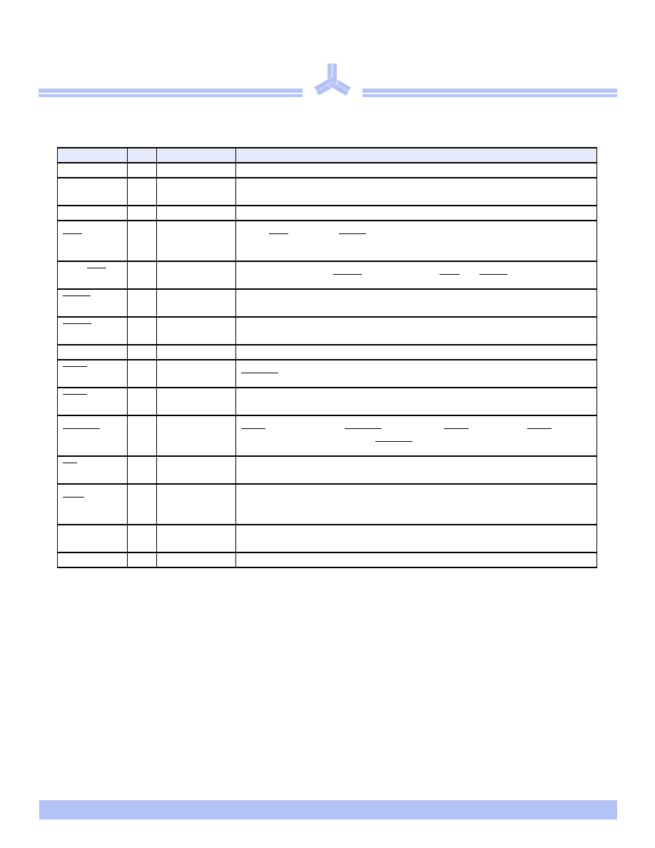
Signal descriptions
Signal
I/O
Properties
Description
CLK
I
CLOCK
Clock. All inputs except OE, ZZ, LBO are synchronous to this clock.
A,A0,A1
I
SYNC
Address. Sampled when all chip enables are active and ADSC or ADSP are
asserted.
DQ[a,b]
I/O
SYNC
Data. Driven as output when the chip is enabled and OE is active.
CE0
I
SYNC
Master chip enable. Sampled on clock edges when ADSP or ADSC is active.
When CE0 is inactive, ADSP is blocked. Refer to the Synchronous Truth Table for
more information.
CE1, CE2
I
SYNC
Synchronous chip enables. Active HIGH and active LOW, respectively. Sampled
on clock edges when ADSC is active or when CE0 and ADSP are active.
ADSP
I
SYNC
Address strobe (processor). Asserted LOW to load a new address or to enter
standby mode.
ADSC
I
SYNC
Address strobe (controller). Asserted LOW to load a new address or to enter
standby mode.
ADV
I
SYNC
Burst advance. Asserted LOW to continue burst read/write.
GWE
I
SYNC
Global write enable. Asserted LOW to write all 18 bits. When HIGH, BWE and
BW[a,b] control write enable.
BWE
I
SYNC
Byte write enable. Asserted LOW with GWE = HIGH to enable effect of BW[a,b]
inputs.
BW[a,b]
I
SYNC
Write enables. Used to control write of individual bytes when GWE = HIGH and
BWE = LOW. If any of BW[a,b] is active with GWE = HIGH and BWE = LOW
the cycle is a write cycle. If all BW[a,b] are inactive, the cycle is a read cycle.
OE
I
ASYNC
Asynchronous output enable. I/O pins are driven when OE is active and the chip is
in read mode.
LBO
I
STATIC
Selects Burst mode. When tied to V
DD
or left floating, device follows interleaved
Burst order. When driven Low, device follows linear Burst order. This signal is
internally pulled High.
ZZ
I ASYNC
Snooze. Places device in low power mode; data is retained. Connect to GND if
unused.
NC
-
-
No connect
Document Outline