Äîêóìåíòàöèÿ è îïèñàíèÿ www.docs.chipfind.ru
January 2005
Copyright © Alliance Semiconductor. All rights reserved.
®
AS7C251MNTD32A
AS7C251MNTD36A
1/17/05, V 1.2
Alliance Semiconductor
P. 1 of 18
2.5V 1M × 32/36 Pipelined SRAM with NTD
TM
Features
· Organization: 1,048,576 words × 32 or 36 bits
· NTD
TM
architecture for efficient bus operation
· Fast clock speeds to 200 MHz
· Fast clock to data access: 3.2/3.5/3.8 ns
· Fast OE access time:
3.2/3.5/3.8 ns
· Fully synchronous operation
· pipelined mode
· Common data inputs and data outputs
· Asynchronous output enable control
· Available in 100-pin TQFP packages
· Byte write enables
· Clock enable for operation hold
· Multiple chip enables for easy expansion
· 2.5V core power supply
· Self-timed write cycles
· Interleaved or linear burst modes
· Snooze mode for standby operation
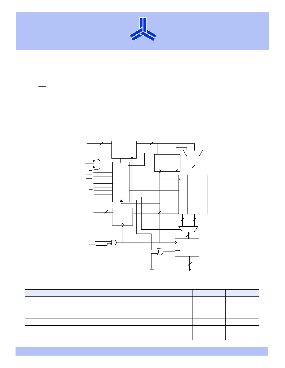
Logic block diagram
Selection guide
-200
-166
-133
Units
Minimum cycle time
5
6
7.5
ns
Maximum clock frequency
200
166
133
MHz
Maximum clock access time
3.2
3.5
3.8
ns
Maximum operating current
450
400
350
mA
Maximum standby current
170
150
140
mA
Maximum CMOS standby current (DC)
90
90
90
mA
Wr
i
t
e
B
u
f
f
e
r
Address
D
Q
CLK
register
Output
Register
DQ[a,b,c,d]
20
20
CLK
CE0
CE1
CE2
A[19:0]
OE
CLK
CEN
Control
CLK
logic
Data
D
Q
CLK
Input
Register
32/36
32/36
OE
1M x 32/36
SRAM
Array
R/W
DQ[a,b,c,d]
BWb
BWd
CLK
Q
D
ADV / LD
LBO
Burst logic
addr. registers
Write delay
20
ZZ
CLK
32/36
32/36
32/36
32/36
BWc
BWa
®
1/17/05, V 1.2
Alliance Semiconductor
P. 2 of 18
AS7C251MNTD32A
AS7C251MNTD36A
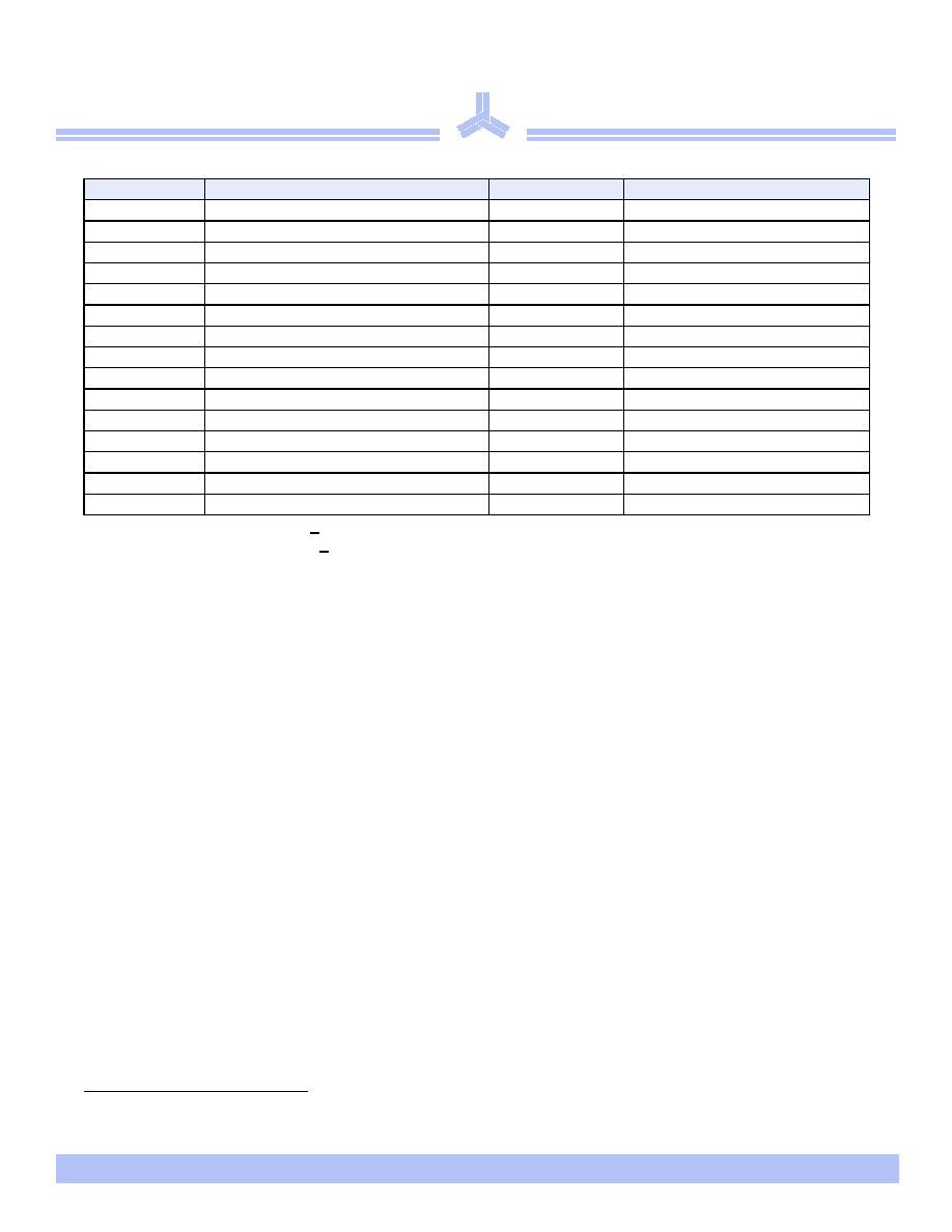
2.5V 32 Mb Synchronous SRAM products list
1,2
1 Core Power Supply: VDD = 2.5V + 0.125V
2 I/O Supply Voltage: VDDQ = 2.5V + 0.125V
PL-SCD
:
Pipelined Burst Synchronous SRAM - Single Cycle Deselect
PL-DCD
:
Pipelined Burst Synchronous SRAM - Double Cycle Deselect
FT
:
Flow-through Burst Synchronous SRAM
NTD
1
-PL
:
Pipelined Burst Synchronous SRAM with NTD
TM
NTD-FT
:
Flow-through Burst Synchronous SRAM with NTD
TM
Org
Part Number
Mode
Speed
2MX18
AS7C252MPFS18A
PL-SCD
200/166/133 MHz
1MX32
AS7C251MPFS32A
PL-SCD
200/166/133 MHz
1MX36
AS7C251MPFS36A
PL-SCD
200/166/133 MHz
2MX18
AS7C252MPFD18A
PL-DCD
200/166/133 MHz
1MX32
AS7C251MPFD32A
PL-DCD
200/166/133 MHz
1MX36
AS7C251MPFD36A
PL-DCD
200/166/133 MHz
2MX18
AS7C252MFT18A
FT
7.5/8.5/10 ns
1MX32
AS7C251MFT32A
FT
7.5/8.5/10 ns
1MX36
AS7C251MFT36A
FT
7.5/8.5/10 ns
2MX18
AS7C252MNTD18A
NTD-PL
200/166/133 MHz
1MX32
AS7C251MNTD32A
NTD-PL
200/166/133 MHz
1MX36
AS7C251MNTD36A
NTD-PL
200/166/133 MHz
2MX18
AS7C252MNTF18A
NTD-FT
7.5/8.5/10 ns
1MX32
AS7C251MNTF32A
NTD-FT
7.5/8.5/10 ns
1MX36
AS7C251MNTF36A
NTD-FT
7.5/8.5/10 ns
1. NTD: No Turnaround Delay. NTD
TM
is a trademark of Alliance Semiconductor Corporation. All trademarks mentioned in this document are the property
of their respective owners.
®
1/17/05, V 1.2
Alliance Semiconductor
P. 3 of 18
AS7C251MNTD32A
AS7C251MNTD36A
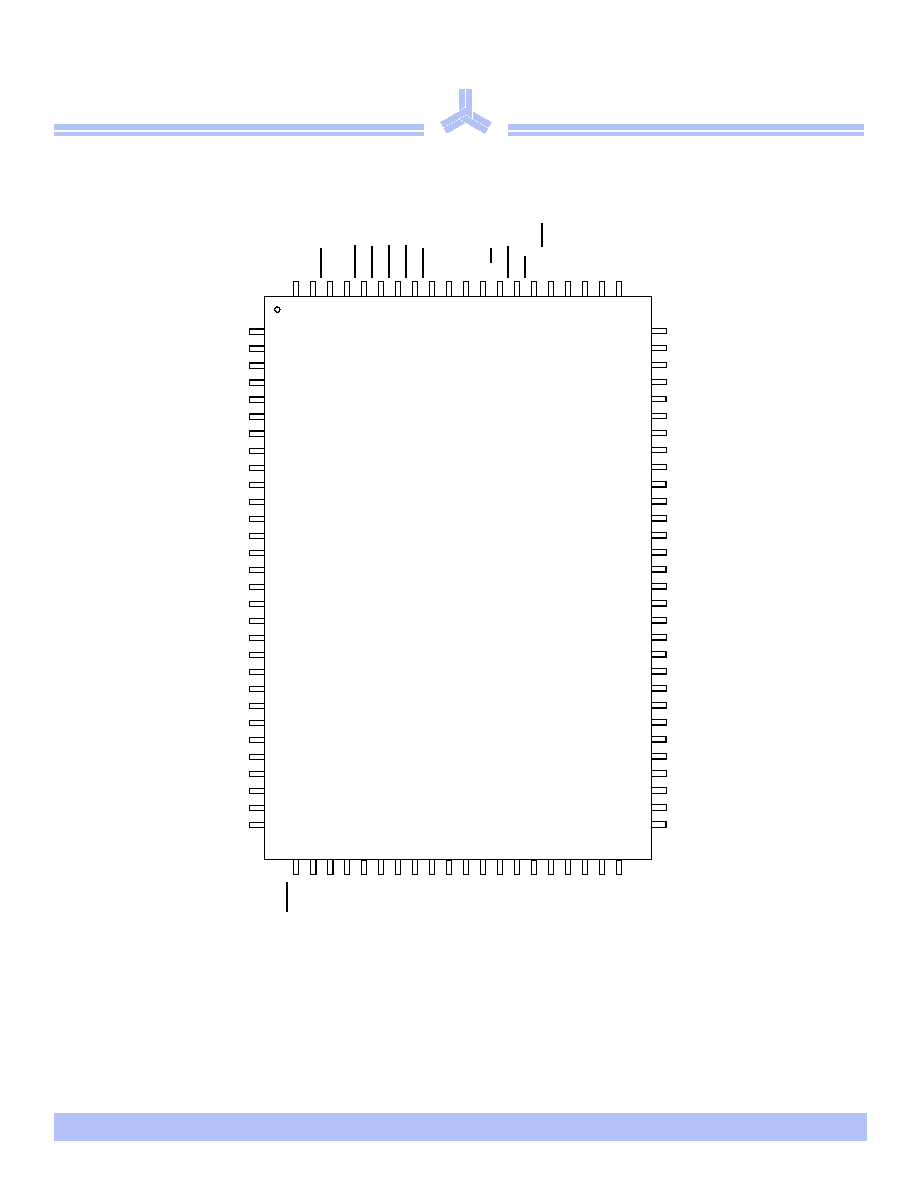
Pin assignment
100-pin TQFP - top view
1
2
3
4
5
6
7
8
9
10
11
12
13
14
15
16
17
18
19
20
21
22
23
24
25
26
27
28
29
30
80
79
78
77
76
75
74
73
72
71
70
69
68
67
66
65
64
63
62
61
60
59
58
57
56
55
54
53
52
51
LBO
A
A
A
A
A1 A0
NC
NC
V
SS
V
DD
NC
A
A
A
A
A
A
A
31
32
33
34
35
36
37
38
39
40
41
42
43
44
45
46
47
48
49
50
100
99
98
97
96
95 94
93
92
91
90
89 88
87
86
85
84
83 82
81
A A
CE0
CE1
BWd
BWc
BWb
BW
a
CE2
V
DD
V
SS
CLK
R/W
CEN
OE
ADV/LD
A
A
A
TQFP 14 x 20mm
A
NC/DQPc
DQc0
DQc1
V
DDQ
V
SSQ
DQc2
DQc3
DQc4
DQc5
V
SSQ
V
DDQ
DQc6
DQc7
V
DD
V
DD
NC
V
SS
DQd0
DQd1
V
DDQ
V
SSQ
DQd2
DQd3
DQd4
DQd5
V
SSQ
V
DDQ
DQd6
DQd7
NC/DQPd
DQPb/NC
DQb7
DQb6
V
DDQ
V
SSQ
DQb5
DQb4
DQb3
DQb2
V
SSQ
V
DDQ
DQb1
DQb0
V
SS
ZZ
DQa7
DQa6
V
DDQ
V
SSQ
DQa5
DQa4
DQa3
DQa2
V
SSQ
V
DDQ
DQa1
DQa0
DQPa/NC
V
DD
NC
Note: For pins 1, 30, 51, and 80, NC applies to the x32 configuration. DQPn applies to the x36 configuration.
A
®
1/17/05, V 1.2
Alliance Semiconductor
P. 4 of 18
AS7C251MNTD32A
AS7C251MNTD36A
Functional description
The AS7C251MNTD32A/36A family is a high performance CMOS 32 Mbit synchronous Static Random Access Memory (SRAM)
organized as 1,048,576 words × 32 or 36 bits and incorporates a LATE LATE Write.
This variation of the 32Mb+ synchronous SRAM uses the No Turnaround Delay (NTD
TM
) architecture, featuring an enhanced write
operation that improves bandwidth over pipelined burst devices. In a normal pipelined burst device, the write data, command, and address
are all applied to the device on the same clock edge. If a read command follows this write command, the system must wait for two 'dead'
cycles for valid data to become available. These dead cycles can significantly reduce overall bandwidth for applications requiring random
access or read-modify-write operations.
NTD
TM
devices use the memory bus more efficiently by introducing a write latency which matches the two-cycle pipelined or one-cycle
flow-through read latency. Write data is applied two cycles after the write command and address, allowing the read pipeline to clear. With
NTD
TM
, write and read operations can be used in any order without producing dead bus cycles.
Assert R/W low to perform write cycles. Byte write enable controls write access to specific bytes, or can be tied low for full 32/36 bit writes.
Write enable signals, along with the write address, are registered on a rising edge of the clock. Write data is applied to the device two clock
cycles later. Unlike some asynchronous SRAMs, output enable OE does not need to be toggled for write operations; it can be tied low for
normal operations. Outputs go to a high impedance state when the device is de-selected by any of the three chip enable inputs. In pipelined
mode, a two cycle deselect latency allows pending read or write operations to be completed.
Use the ADV (burst advance) input to perform burst read, write and deselect operations. When ADV is high, external addresses, chip select, R/W
pins are ignored, and internal address counters increment in the count sequence specified by the LBO control. Any device operations, including
burst, can be stalled using the CEN=1, the clock enable input.
The AS7C251MNTD32A/36A operates with a 2.5V ± 5% power supply for the device core (V
DD
). These devices are available in a 100-pin
TQFP package.
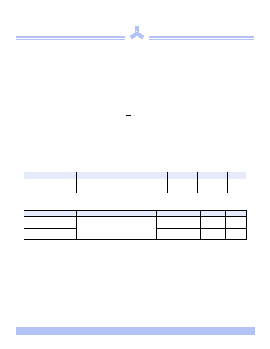
TQFP Capacitance
*Guaranteed not tested
TQFP thermal resistance
Parameter
Symbol
Test conditions
Min
Max
Unit
Input capacitance
C
IN
*
V
in
= 0V
-
5
pF
I/O capacitance
C
I/O
*
V
in
= V
out
= 0V
-
7
pF
Description
Conditions
Symbol
Typical
Units
Thermal resistance
(junction to ambient)
1
1 This parameter is sampled
Test conditions follow standard test methods
and procedures for measuring thermal
impedance, per EIA/JESD51
1layer
JA
40
°C/W
4layer
JA
22
°C/W
Thermal resistance
(junction to top of case)
1
JC
8
°C/W
®
1/17/05, V 1.2
Alliance Semiconductor
P. 5 of 18
AS7C251MNTD32A
AS7C251MNTD36A
Signal descriptions
Snooze Mode
SNOOZE MODE is a low current, power-down mode in which the device is deselected and current is reduced to I
SB2
. The duration of
SNOOZE MODE is dictated by the length of time the ZZ is in a High state.
The ZZ pin is an asynchronous, active high input that causes the device to enter SNOOZE MODE.
When the ZZ pin becomes a logic High, I
SB2
is guaranteed after the time t
ZZI
is met. After entering SNOOZE MODE, all inputs except ZZ
is disabled and all outputs go to High-Z. Any operation pending when entering SNOOZE MODE is not guaranteed to successfully complete.
Therefore, SNOOZE MODE (READ or WRITE) must not be initiated until valid pending operations are completed. Similarly, when exiting
SNOOZE MODE during t
PUS
, only a DESELECT or READ cycle should be given while the SRAM is transitioning out of SNOOZE
MODE.
Signal
I/O
Properties Description
CLK
I
CLOCK
Clock. All inputs except OE, LBO, and ZZ are synchronous to this clock.
CEN
I
SYNC
Clock enable. When de-asserted high, the clock input signal is masked.
A, A0, A1
I
SYNC
Address. Sampled when all chip enables are active and ADV/LD is asserted.
DQ[a,b,c,d]
I/O
SYNC
Data. Driven as output when the chip is enabled and OE is active.
CE0, CE1,
CE2
I
SYNC
Synchronous chip enables. Sampled at the rising edge of CLK, when ADV/LD is asserted.
Are ignored when ADV/LD is high.
ADV/LD
I
SYNC
Advance or Load. When sampled high, the internal burst address counter will increment in
the order defined by the LBO input value. When low, a new address is loaded.
R/W
I
SYNC
A high during LOAD initiates a READ operation. A low during LOAD initiates a WRITE
operation. Is ignored when ADV/LD is high.
BW[a,b,c,d]
I
SYNC
Byte write enables. Used to control write on individual bytes. Sampled along with WRITE
command and BURST WRITE.
OE
I
ASYNC
Asynchronous output enable. I/O pins are not driven when OE is inactive.
LBO
I
STATIC
Selects Burst mode. When tied to V
DD
or left floating, device follows interleaved Burst order. When
driven Low, device follows linear Burst order. This signal is internally pulled High.
ZZ
I
ASYNC
Snooze. Places device in low power mode; data is retained. Connect to GND if unused.
NC
-
-
No connect
Document Outline