Äîêóìåíòàöèÿ è îïèñàíèÿ www.docs.chipfind.ru
January 2001
Advance Information
Copyright © Alliance Semiconductor. All rights reserved.
®
AS7C1026A
AS7C31026A
5V/3.3V 64K X 16 CMOS SRAM
2/6/01; V.0.9
Alliance Semiconductor
P. 1 of 9
Features
· AS7C1026A (5V version)
· AS7C31026A (3.3V version)
· Industrial and commercial versions
· Organization: 65,536 words × 16 bits
· Center power and ground pins for low noise
· High speed
- 10/12/15/20 ns address access time
- 3/3/4/5 ns output enable access time
· Low power consumption: ACTIVE
- 660 mW (AS7C1026A) / max @ 10 ns
- 324 mW (AS7C31026A) / max @ 10 ns
· Low power consumption: STANDBY
- 55 mW (AS7C1026A) / max CMOS I/O
- 36 mW (AS7C31026A) / max CMOS I/O
· Latest 6T 0.25u CMOS technology
· 2.0V data retention
· Easy memory expansion with CE, OE inputs
· TTL-compatible, three-state I/O
· JEDEC standard packaging
- 44-pin 400 mil SOJ
- 44-pin 400 mil TSOP II
- 48-ball 6 mm × 8 mm CSP mBGA
· ESD protection
2000 volts
· Latch-up current
200 mA
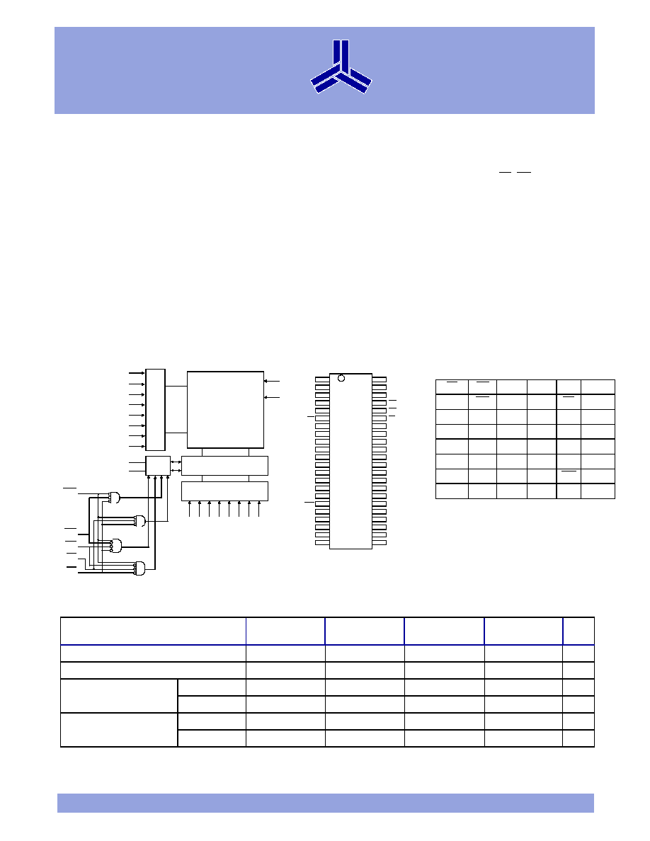
Logic block diagram
64K × 16
Array
OE
CE
WE
Column decoder
Ro
w de
c
o
de
r
A0
A1
A2
A3
A4
A5
A7
V
CC
GND
A8
A9
A10
A11
A12
A13
A14
A15
Control circuit
I/O0I/O7
I/O8I/O15
UB
LB
I/O
buffer
A6
Pin arrangement
5
6
7
8
9
10
11
12
13
14
15
16
17
18
19
20
I/O13
I/O12
GND
V
CC
I/O11
I/O10
I/O9
I/O8
NC
A8
A9
A10
A11
NC
A0
CE
I/O0
I/O1
I/O2
I/O3
V
CC
GND
I/O4
I/O5
I/O6
I/O7
WE
A15
A14
A13
44-Pin SOJ, TSOP II (400 mil)
21
22
A12
NC
UB
LB
I/O15
I/O14
2
A3
3
A2
4
A1
1
A4
40
39
38
37
36
35
34
33
32
31
30
29
28
27
26
25
24
23
43
42
41
44
A6
A7
OE
A5
A
S
7
C
10
26
A
A
S
7
C
31
02
6A
Selection guide
AS7C1026A-10
AS7C31026A-10
AS7C1026A-12
AS7C31026A-12
AS7C1026A-15
AS7C31026A-15
AS7C1026A-20
AS7C31026A-20
Unit
Maximum address access time
10
12
15
20
ns
Maximum output enable access time
3
3
4
5
ns
Maximum operating current
AS7C1026A
120
110
100
100
mA
AS7C31026A
90
80
80
80
mA
Maximum CMOS standby
current
AS7C1026A
10
10
10
15
mA
AS7C31026A
10
10
10
15
mA
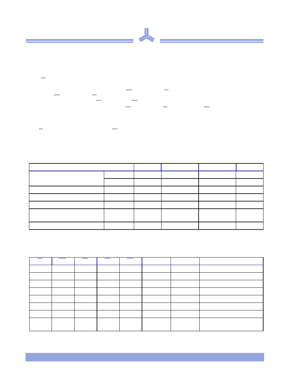
48-CSP mini Ball-Grid-Array Package
1
2
3
4
5
6
A
LB
OE
A
0
A
1
A
2
NC
B
I/O8
UB
A3
A4
CE
I/O0
C
I/O9 I/O10
A5
A6
I/O1 I/O2
D
V
SS
I/O11
NC
A7
I/O3
V
DD
E
V
DD
I/O12
NC
NC I/O4
V
SS
F
I/O14 I/O13 A14
A15 I/O5 I/O6
G I/O15
NC
A12
A13
WE
I/O7
H
NC
A8
A9
A10
A11
NC
®
AS7C1026A
AS7C31026A
2/6/01; V.0.9
Alliance Semiconductor
P. 2 of 9
Functional description
The AS7C1026A and AS7C31026A are high-performance CMOS 1,048,576-bit Static Random Access Memory (SRAM) devices organized as
65,536 words × 16 bits. They are designed for memory applications where fast data access, low power, and simple interfacing are desired.
Equal address access and cycle times (t
AA
, t
RC
, t
WC
) of 10/12/15/20 ns with output enable access times (t
OE
) of 3/3/4/5 ns are ideal for
high-performance applications.
When CE is high the devices enter standby mode. The AS7C1026A is guaranteed not to exceed 55 mW power consumption in CMOS
standby mode. The devices also offer 2.0V data retention.
A write cycle is accomplished by asserting write enable (WE) and chip enable (CE). Data on the input pins I/O0I/O15 is written on the
rising edge of WE (write cycle 1) or CE (write cycle 2). To avoid bus contention, external devices should drive I/O pins only after outputs
have been disabled with output enable (OE) or write enable (WE).
A read cycle is accomplished by asserting output enable (OE) and chip enable (CE), with write enable (WE) high. the chips drive I/O pins
with the data word referenced by the input address. When either chip enable or output enable is inactive, or write enable is active, output
drivers stay in high-impedance mode.
The devices provide multiple center power and ground pins, and separate byte enable controls, allowing individual bytes to be written and
read. LB controls the lower bits, I/O0I/O7, and UB controls the higher bits, I/O8I/O15.
All chip inputs and outputs are TTL-compatible, and operation is from a single 5V supply (AS7C1026A) or 3.3V supply (AS7C31026A). the
device is packaged in common industry standard packages. Chip scale BGA packaging, easy to use in manufacturing, provides the smallest
possible footprint. This 48-ball JEDEC-registered package has a ball pitch of 0.75 mm and external dimensions of 8 mm × 6 mm.
Absolute maximum ratings
Note: Stresses greater than those listed under Absolute Maximum Ratings may cause permanent damage to the device. This is a stress rating only and functional
operation of the device at these or any other conditions outside those indicated in the operational sections of this specification is not implied. Exposure to
absolute maximum rating conditions for extended periods may affect reliability.
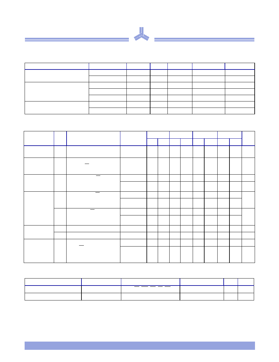
Truth table
Key:
H = High, L = Low, X = don't care.
Parameter
Symbol
Min
Max
Unit
Voltage on V
CC
relative to GND
AS7C1026A
V
t1
0.50
+7.0
V
AS7C31026A
V
t1
0.50
+5.0
V
Voltage on any pin relative to GND
Both
V
t2
0.50
V
CC
+0.50
V
Power dissipation
Both
P
D
1.0
W
Storage temperature (plastic)
Both
T
stg
65
+150
°
C
Ambient temperature with VCC
applied
Both
T
bias
55
+125
°
C
DC current into outputs (low)
Both
I
OUT
20
mA
CE
WE
OE
LB
UB
I/O0I/O7
I/O8I/O15
Mode
H
X
X
X
X
High Z
High Z
Standby (I
SB
), I
SBI
)
L
H
L
L
H
D
OUT
High Z
Read I/O0I/O7 (I
CC
)
L
H
L
H
L
High Z
D
OUT
Read I/O8I/O15 (I
CC)
L
H
L
L
L
D
OUT
D
OUT
Read I/O0I/O15 (I
CC
)
L
L
X
L
L
D
IN
D
IN
Write I/O0I/O15 (I
CC
)
L
L
X
L
H
D
IN
High Z
Write I/O0I/O7 (I
CC
)
L
L
X
H
L
High Z
D
IN
Write I/O8I/O15 (I
CC
)
L
L
H
X
H
X
X
H
X
H
High Z
High Z
Output disable (I
CC
)
®
AS7C1026A
AS7C31026A
2/6/01; V.0.9
Alliance Semiconductor
P. 3 of 9
Recommended operating conditions
V
IL
min. = 3.0V for pulse width less than t
RC
/2.
DC operating characteristics (over the operating range)
1
Capacitance (f = 1MHz, T
a
= 25
°
C, V
CC
= NOMINAL)
2
Parameter
Device
Symbol
Min
Nominal
Max
Unit
Supply voltage
AS7C1026A
V
CC
4.5
5.0
5.5
V
AS7C31026A
V
CC
3.0
3.3
3.6
V
Input voltage
AS7C1026A
V
IH
2.2
V
CC
+ 0.5
V
AS7C31026A
V
IH
2.0
V
CC
+ 0.5
V
Both
V
IL
0.5
0.8
V
Ambient operating temperature
commercial
T
A
0
70
o
C
industrial
T
A
40
85
o
C
Parameter
Sym
Test conditions
Device
-10
-12
-15
-20
Unit
Min Max Min Max Min
Max
Min
Max
Input leakage
current
|
I
LI
|
V
CC
= Max
V
IN
= GND to V
CC
Both
1
1
1
1
µA
Output leakage
current
|
I
LO
|
V
CC
= Max
CE = V
IH
,
V
OUT
= GND to V
CC
Both
1
1
1
1
µA
Operating power
supply current
I
CC
V
CC
= Max, CE
V
IL
outputs open,
f = f
Max
= 1/t
RC
AS7C1026A
120
110
100
100
mA
AS7C31026A
90
80
80
80
mA
Standby
power supply
current
I
SB
V
CC
= Max, CE
V
IL
,
outputs open,
f = f
Max
= 1/t
RC
AS7C1026A
30
25
20
20
mA
AS7C31026A
30
25
20
20
I
SB1
V
CC
= Max, CE
V
CC
0.2V,
V
IN
GND + 0.2V or
V
IN
V
CC
0.2V, f = 0
AS7C1026A
10
10
10
15
mA
AS7C31026A
10
10
10
15
Output
voltage
V
OL
I
OL
= 8 mA, V
CC
= Min
AS7C1026A
0.4
0.4
0.4
0.4
V
V
OH
I
OH
= 4 mA, V
CC
= Min
AS7C31026A
2.4
2.4
2.4
2.4
V
Data retention
current
I
CCDR
V
CC
= 2.0V
CE
V
CC
0.2V
V
IN
V
CC
0.2V or
V
IN
0.2V
AS7C1026A
1
1
1
5
mA
AS7C31026A
1
1
1
5
mA
Parameter
Symbol
Signals
Test conditions
Max
Unit
Input capacitance
C
IN
A, CE, WE, OE, LB, UB
V
IN
= 0V
5
pF
I/O capacitance
C
I/O
I/O
V
IN
= V
OUT
= 0V
7
pF
®
AS7C1026A
AS7C31026A
2/6/01; V.0.9
Alliance Semiconductor
P. 4 of 9
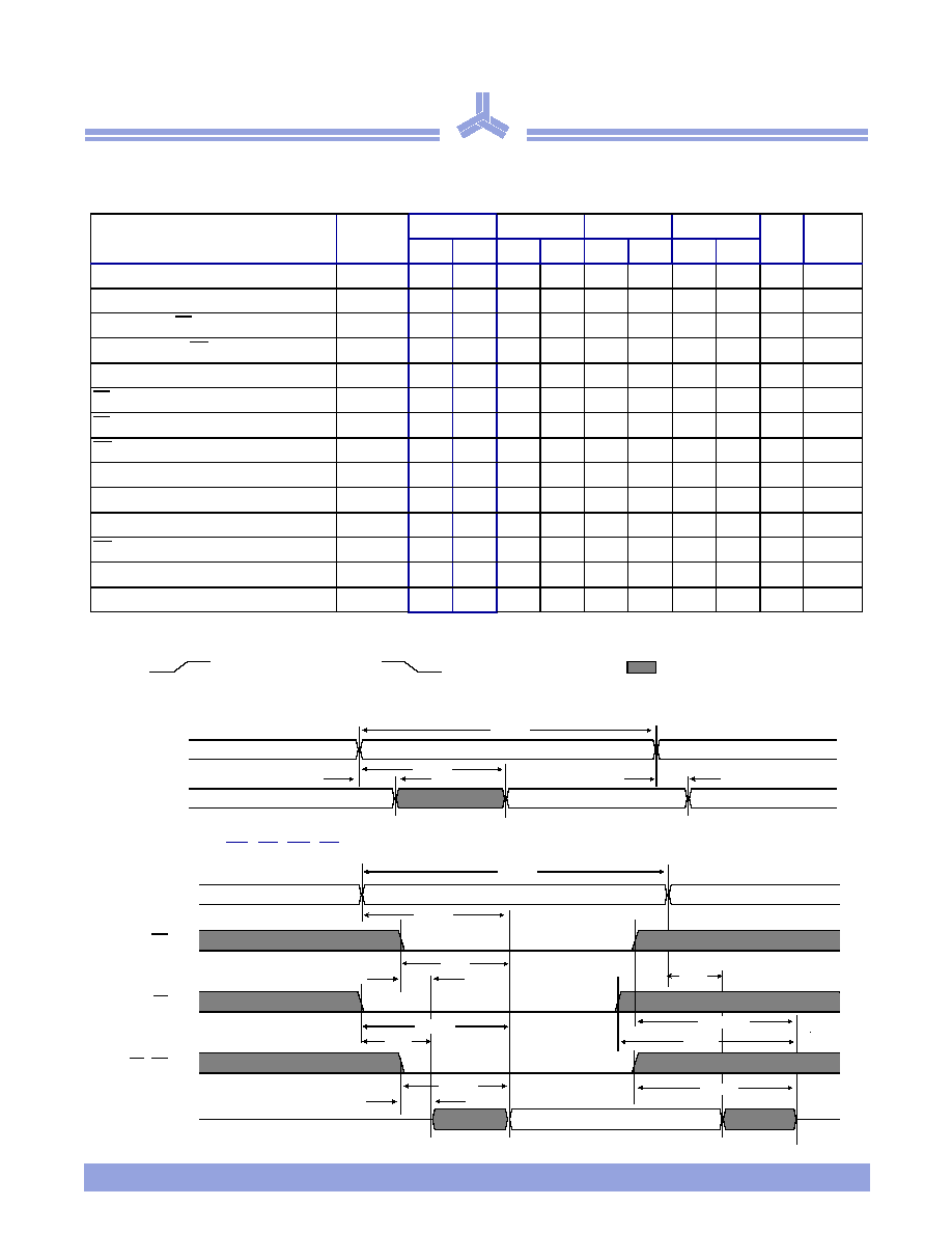
Read cycle (over the operating range)
3,9
Key to switching waveforms
Read waveform 1 (address controlled)
3,6,7,9
Read waveform 2 (OE, CE, UB, LB controlled)
3,6,8,9
Parameter
Symbol
-10
-12
-15
-20
Unit
Notes
Min
Max
Min
Max
Min
Max
Min
Max
Read cycle time
t
RC
10
12
15
20
ns
Address access time
t
AA
10
12
15
20
ns
3
Chip enable (CE) access time
t
ACE
10
12
15
20
ns
3
Output enable (OE) access time
t
OE
3
3
4
5
ns
Output hold from address change
t
OH
2
3
3
3
ns
5
CE Low to output in low Z
t
CLZ
0
0
0
0
ns
4, 5
CE High to output in high Z
t
CHZ
3
3
4
5
ns
4, 5
OE Low to output in low Z
t
OLZ
0
0
0
0
ns
4, 5
Byte select access time
t
BA
3
3
4
5
ns
Byte select Low to low Z
t
BLZ
0
0
0
0
ns
4, 5
Byte select High to high Z
t
BHZ
5
6
6
8
ns
4, 5
OE High to output in high Z
t
OHZ
3
3
4
5
ns
4, 5
Power up time
t
PU
0
0
0
0
ns
4, 5
Power down time
t
PD
10
12
15
20
ns
4, 5
Undefined output/don't care
Falling input
Rising input
t
OH
t
AA
t
RC
t
OH
Data
OUT
Address
Data valid
Previous data valid
Data valid
t
RC
t
AA
t
BLZ
t
BA
t
OE
t
OLZ
t
OH
t
OHZ
t
HZ
t
BHZ
t
ACE
t
LZ
Address
OE
CE
LB, UB
Data
IN
®
AS7C1026A
AS7C31026A
2/6/01; V.0.9
Alliance Semiconductor
P. 5 of 9
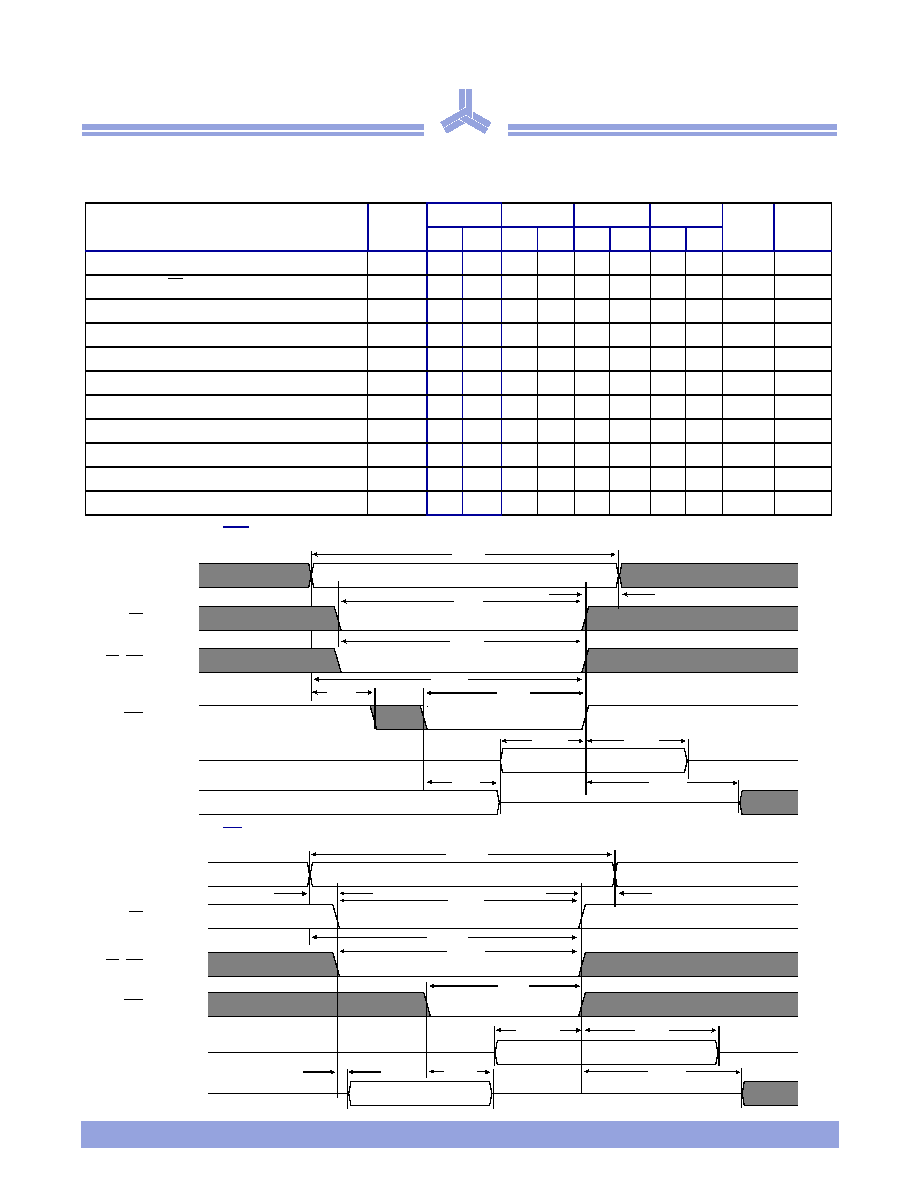
Write cycle (over the operating range)
11
Write waveform 1 (WE controlled)
10,11
Write waveform 2 (CE controlled)
10,11
Parameter
Symbol
-10
-12
-15
-20
Unit
Notes
Min Max Min Max Min Max Min Max
Write cycle time
t
WC
10
12
15
20
ns
Chip enable (CE) to write end
t
CW
8
10
12
12
ns
Address setup to write end
t
AW
8
9
10
12
ns
Address setup time
t
AS
0
0
0
0
ns
Write pulse width
t
WP
7
8
9
12
ns
Address hold from end of write
t
AH
0
0
0
0
ns
Data valid to write end
t
DW
5
6
8
10
ns
Data hold time
t
DH
0
0
0
0
ns
5
Write enable to output in high Z
t
WZ
6
6
6
8
ns
4, 5
Output active from write end
t
OW
1
1
1
2
ns
4, 5
Byte select low to end of write
t
BW
8
10
12
12
ns
Address
CE
LB, UB
WE
Data
IN
Data
OUT
t
WC
t
CW
t
BW
t
AW
t
AS
t
WP
t
DW
t
DH
t
OW
t
WZ
t
WR
Data undefined
high Z
Data valid
Address
CE
LB, UB
WE
Data
IN
t
WC
t
CW
t
BW
t
WP
t
DW
t
DH
t
OW
t
WZ
t
WR
Data
OUT
Data undefined
high Z
high Z
t
AS
t
AW
Data valid
t
CLZ
Document Outline