 | –≠–ª–µ–∫—Ç—Ä–æ–Ω–Ω—ã–π –∫–æ–º–ø–æ–Ω–µ–Ω—Ç: 3946 | –°–∫–∞—á–∞—Ç—å:  PDF PDF  ZIP ZIP |

Data Sheet
29319.150
3946
Half-Bridge Power MOSFET Controller
The A3946 is designed specifi cally for ap pli ca tions that require
high power unidirectional dc motors, three-phase brushless dc motors, or
other inductive loads. The A3946 provides two high-current gate drive
outputs that are capable of driving a wide range of power N-channel
MOSFET
s. The high-side gate driver switches an N-channel
MOSFET
that controls current to the load, while the low-side gate driver switches
an N-channel
MOSFET
as a synchronous rectifi er.
A bootstrap capacitor provides the above-battery supply voltage
required for N-channel MOSFETs. An internal charge pump for the
high side allows for dc (100% duty cycle) operation of the half-bridge.
The A3946 is available in a choice of two power pack ag es: a
16-lead
SOIC
with copper batwing power tab (part number suffi x LB),
and a 16-lead
TSSOP
with ex posed thermal pad (suffi x LP).
On-chip charge pump for 7 V minimum input supply voltage
High-current gate drive for driving a wide range of
N-channel
MOSFET
s
Bootstrapped gate drive with charge pump for 100% duty cycle
Overtemperature protection
Undervoltage protection
≠40∫C to 135∫C ambient operation
Always order by complete part number:
Load Supply Voltage, V
BB
............................. 60 V
Logic Inputs ..................................≠0.3 V to 6.5 V
Pin S................................................≠4 V to 60 V
Pin GH ...........................................≠4 V to 75 V
Pin BOOT..... ................................≠0.6 V to 75 V
Pin DT ........................................................ V
REF
Pin VREG ......................................≠0.6 V to 15 V
Package Thermal Resistance, R
JA
A3946KLB..................................... 48
∞C/W
1
A3946KLB..................................... 38
∞C/W
2
A3946KLP ..................................... 44
∞C/W
1
A3946KLP ..................................... 34
∞C/W
2
Operating Temperature Range, T
A
.. ≠40
∞C to +135∞C
Junction Temperature, T
J
...........................+150
∞C
Storage Temperature Range, T
S
....-55
∞C to +150∞C
Notes:
1. Measured on a two-sided PCB with 3 in.
2
of
2 oz. copper.
2. Measured on JEDEC standard High-K board.
AB SO LUTE MAX I MUM RAT INGS
A3946KLB SOIC
A3946KLP TSSOP with Exposed Thermal Pad
3
4
5
6
7
8
2
1
14
13
12
11
10
9
15
16
VREG
CP2
CP1
PGND
GL
S
GH
BOOT
VBB
VREF
DT
LGND
RESET
IN2
IN1
~FAULT
FEATURES
Scale 1:1
Scale 1:1
3
4
5
6
7
8
2
1
14
13
12
11
10
9
15
16
VREG
CP2
CP1
PGND
GL
S
GH
BOOT
VBB
VREF
DT
LGND
RESET
IN2
IN1
~FAULT
Part Number
Package
A3946KLB
A3946KLP
16-Lead SOIC; Copper Batwing Power Tab
16-Lead TSSOP; Exposed Thermal Pad

2
Worcester, Massachusetts 01615-0036 (508) 853-5000
115 Northeast Cutoff, Box 15036
www.allegromicro.com
Data Sheet
29319.150
3946
Half-Bridge Power MOSFET Controller
Functional Block Diagram
Control Logic Table
IN1
IN2
DT Pin
RESET
GH
GL
Function
X
X
X
0
Z
Z
Sleep mode
0
0
R
DEAD
- LGND
1
L
H
Low-side FET ON following dead time
0
1
R
DEAD
- LGND
1
L
L
All OFF
1
0
R
DEAD
- LGND
1
L
L
All OFF
1
1
R
DEAD
- LGND
1
H
L
High-side FET ON following dead time
0
0
VREF
1
L
L
All OFF
0
1
VREF
1
L
H
Low-side FET ON
1
0
VREF
1
H
L
High-side FET ON
1
1
VREF
1
H
H
CAUTION: High-side and low-side FETs ON
VBB
VREG
C
BOOT
+VBAT
+5 Vref
Charge
Pump
BOOT
GH
S
GL
LGND
VREG
CP1
CP2
Charge
Pump
RESET
Protection
VREG Undervoltage
Overtemperature
UVLOBOOT
IN2
~FAULT
DT
Control
Logic
Turn-On
Delay
IN1
R
DEAD
VREF
VREF
Bootstrap
UVLO
10
k
C
REG
C1
0.47 uF, X7R
V rated to VBAT
R
GATE
R
GATE
I
LIM
PGND
High Side
Driver
Low Side
Driver
C2
0.47 uF, X7R
V rated to VBAT
0.1 uF
X7R
10 V
P
L
P
L
L
L
L
L
L
P
P
L
P
P

3
Worcester, Massachusetts 01615-0036 (508) 853-5000
115 Northeast Cutoff, Box 15036
www.allegromicro.com
Data Sheet
29319.150
3946
Half-Bridge Power MOSFET Controller
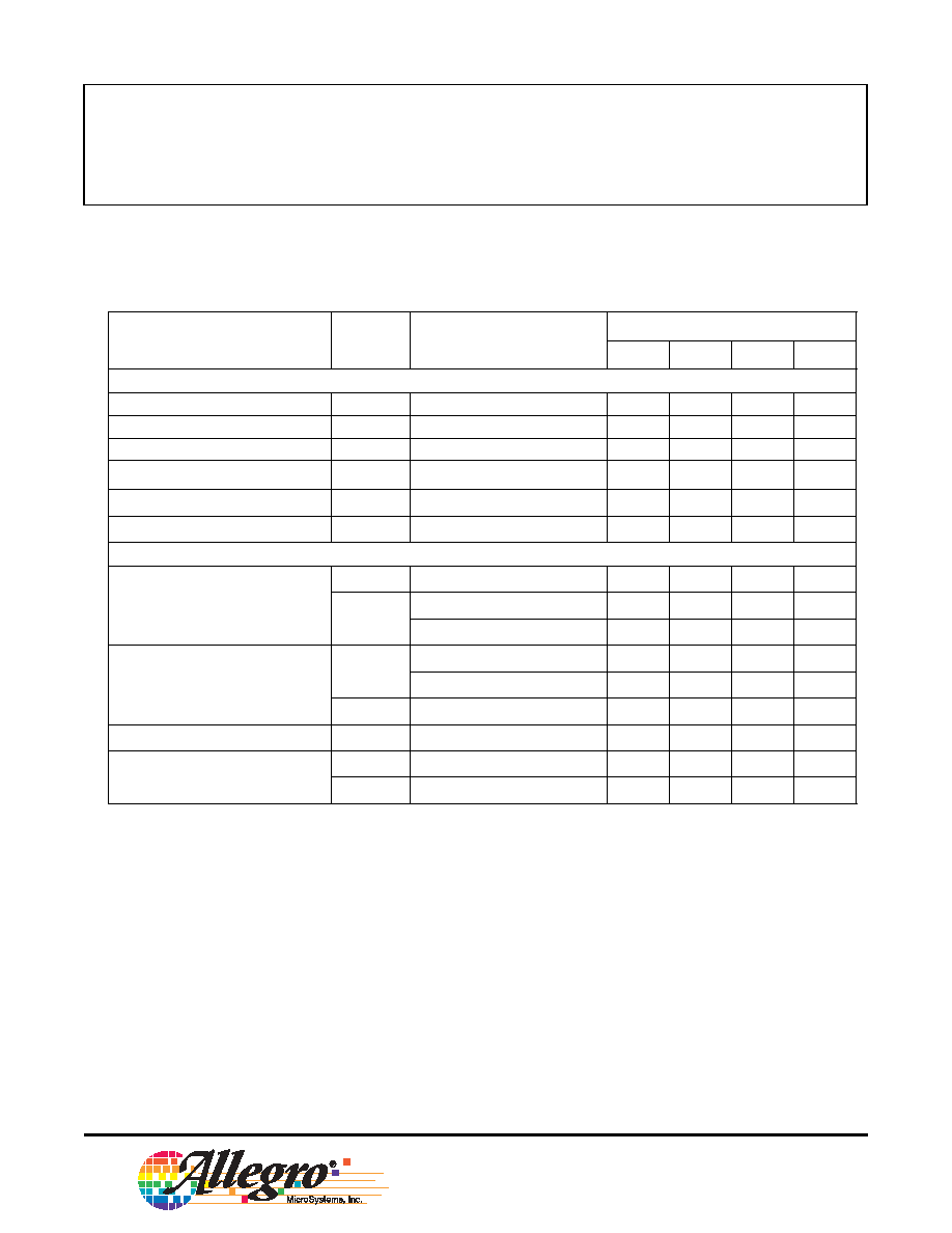
ELECTRICAL CHARACTERISTICS at T
A
= ≠40 to +135∞C, V
BB
= 7 to 60 V (unless otherwise noted)
Characteristics
Symbol
Test Conditions
Limits
Min.
Typ.
Max.
Units
V
BB
Quiescent Current
I
VBB
RESET = High, Outputs Low
≠
3
6
mA
RESET = Low
≠
≠
10
µA
VREG Output Voltage
V
REG
V
BB
> 7.75 V, I
reg
= 0 mA to 15 mA
12.0
13
13.5
V
V
BB
= 7 V to 7.75 V, I
reg
= 0 mA to 15 mA
11.0
≠
13.5
V
Charge Pump Frequency
F
CP
CP1, CP2
≠
62.5
≠
kHz
VREF Output Voltage
V
REF
I
REF
4 mA, C
REF
= 0.1 µF
4.5
≠
5.5
V
Gate Output Drive
Turn On Time
t
rise
C
LOAD
= 3300 pF, 20% to 80%
≠
60
100
ns
Turn Off Time
t
fall
C
LOAD
= 3300 pF, 80% to 20%
≠
40
80
ns
Pullup On Resistance
R
DSUP
T
j
= 25
∞C
≠
4
≠
T
j
= 135
∞C
≠
6
≠
Pulldown On Resistance
R
DSDOWN
T
j
= 25
∞C
≠
2
≠
T
j
= 135
∞C
≠
3
≠
Short Circuit Current ≠
Source
≠
t
pw
< 10 µs
800
≠
≠
mA
Short Circuit Current ≠
Sink
≠
t
pw
< 10 µs
1000
≠
≠
mA
GH Output Voltage
V
GH
t
pw
< 10 µs, Bootstrap Capacitor fully charged
V
REG
≠ 1.5
≠
≠
V
GL Output Voltage
V
GL
≠
V
REG
≠ 0.2
≠
≠
V
Timing
Dead Time (Delay from
Turn Off to Turn On)
t
DEAD
R
dead
= 5 k
200
350
500
ns
R
dead
= 100 k
5
6
7
µs
Propagation Delay
t
PD
Logic input to unloaded GH, GL. DT = VREF
≠
≠
150
ns
4
Worcester, Massachusetts 01615-0036 (508) 853-5000
115 Northeast Cutoff, Box 15036
www.allegromicro.com
Data Sheet
29319.150
3946
Half-Bridge Power MOSFET Controller
Limits
Characteristics
Symbol
Test Conditions
Min.
Typ.
Max.
Units
Protection
VREG Undervoltage
V
REGON
V
REG
increasing
8.6
9.1
9.6
V
VREG Undervoltage
V
REGOFF
V
REG
decreasing
7.8
8.3
8.8
V
BOOT Undervoltage
V
BSON
V
BOOT
increasing
8
8.75
9.5
V
BOOT Undervoltage
V
BSOFF
V
BOOT
decreasing
7.25
8.0
8.75
V
Thermal Shutdown Temperature
T
JTSD
Temperature increasing
≠
170
≠
∞C
Thermal Shutdown Hysteresis
T
J
Recovery = T
JTSD
≠
T
J
≠
15
≠
∞C
Logic
Input Current
I
IN(1)
IN1 V
IN
/ IN2 V
IN
= 2.0 V
≠
40
100
µA
I
IN(0)
IN1 V
IN
/ IN2 V
IN
= 0.8 V
≠
16
40
µA
RESET pin only
≠
≠
1
µA
Logic Input Voltage
V
IN(1)
IN1 / IN2 logic high
2.0
≠
≠
V
RESET logic high
2.2
≠
≠
V
V
IN(0)
Logic low
≠
≠
0.8
V
Logic Input Hysteresis
≠
All digital inputs
100
≠
300
mV
Fault Output
V
ol
I = 1 mA, fault asserted
≠
≠
400
mV
V
oh
V = 5 V
≠
≠
1
µA
ELECTRICAL CHARACTERISTICS
at T
A
= ≠40 to +135∞C, V
BB
= 7 to 60 V (unless otherwise noted)

5
Worcester, Massachusetts 01615-0036 (508) 853-5000
115 Northeast Cutoff, Box 15036
www.allegromicro.com
Data Sheet
29319.150
3946
Half-Bridge Power MOSFET Controller
VREG. A 13 V output from the on-chip charge pump, used
to power the low-side gate drive circuit directly, provides the
current to charge the bootstrap capacitors for the high-side
gate drive.
The VREG capacitor, C
REG
, must supply the instantaneous
current to the gate of the low-side MOSFET. A 10 µF, 25 V
capacitor should be adequate. This capacitor can be either
electrolytic or ceramic (X7R).
Diagnostics and Protection. The fault output pin,
~FAULT, goes low (i.e., FAULT = 1) when the RESET line
is high and any of the following conditions are present:
∑ Undervoltage conditions on VREG (UVREG) or on the
internal logic supply VREF (UVREF). These conditions
set a latched fault.
∑ A junction temperature > 170∞C (OVERTEMP). This con-
dition sets a latched fault.
∑ An undervoltage on the stored charge of the BOOT capaci-
tor (UVBOOT). This condition does NOT set a latched
fault.
An overtemperature event signals a latched fault, but does
not disable any output drivers, regulators, or logic inputs.
The user must turn off the A3946 (e.g., force the RESET line
low) to prevent damage.
The power FETs are protected from inadequate gate drive
voltage by undervoltage detectors. Either of the regulator
undervoltage faults (UVREG or UVREF) disable both output
drivers until both voltages have been restored. The high-side
driver is also disabled during a UVBOOT fault condition.
Under many operating conditions, both the high-side (GH)
and low-side (GL) drivers may be off, allowing the BOOT
capacitor to discharge (or never become charged) and create
a UVBOOT fault condition, which in turn inhibits the high-
side driver and creates a FAULT = 1. This fault is NOT
latched. To remove this fault, momentarily turn on GL to
charge the BOOT capacitor.
Latched faults may be cleared by a low pulse, 1 to 10 µs
wide, on the RESET line. Throughout that pulse (despite
a possible UVBOOT), FAULT = 0; also the fault latch is
cleared immediately, and remains cleared. If the power is
restored (no UVREG or UVREF), and if no OVERTEMP
fault exists, then the latched fault remains cleared when the
RESET line returns to high. However, FAULT = 1 may still
occur because a UVBOOT fault condition may still exist.
Charge Pump. The A3946 is designed to ac com mo date
a wide range of power supply voltages. The charge pump
output, VREG, is regulated to 13 V nominal.
In all modes, this regulator is current-limited. When V
BB
< 8 V, the charge pump operates as a voltage doubler. When
8 V < V
BB
< 15 V, the charge pump operates as a voltage
doubler/PWM, current-controlled, voltage regulator. When
V
BB
>15 V, the charge pump operates as a PWM, current-con-
trolled, voltage regulator. Effi ciency shifts, from 80% at V
BB
=
7 V, to 20% at V
BB
= 50 V.
CAUTION. Although simple paralleling of VREG supplies
from several A3946s may appear to work correctly, such a
confi guration is NOT recommended. There is no assurance
that one of the regulators will not dominate, taking on all of
the load and back-biasing the other regulators. (For example,
this could occur if a particular regulator has an internal refer-
ence voltage that is higher that those of the other regulators,
which would force it to regulate at the highest voltage.)
Sleep Mode/Power Up. In Sleep Mode, all circuits are
disabled in order to draw minimum current from VBB. When
powering up and leaving Sleep Mode (the RESET line is
high), the gate drive outputs stay disabled and a fault remains
asserted until VREF and VREG pass their undervoltage
thresholds. When powering up, before starting the fi rst boot-
strap charge cycle, wait until t = C
REG
/ 4 (where C
REG
is in
µF, and t is in ns) to allow the charge pump to stabilize.
When powered-up (not in Sleep Mode), if the RESET line
is low for > 10 µs, the A3946 may start to enter Sleep Mode
(V
REF
< 4 V). In that case, ~FAULT = 1 as long as the RESET
line remains low.
If the RESET line is open, the A3946 should go into Sleep
Mode. However, to ensure that this occurs, the RESET line
must be grounded.
Functional Description