| –≠–ª–µ–∫—Ç—Ä–æ–Ω–Ω—ã–π –∫–æ–º–ø–æ–Ω–µ–Ω—Ç: AKD4125 | –°–∫–∞—á–∞—Ç—å:  PDF PDF  ZIP ZIP |
ASAHI KASEI
[AKD4125-A]
<KM078700>
2005/06
- 1 -
GENERAL DESCRIPTION
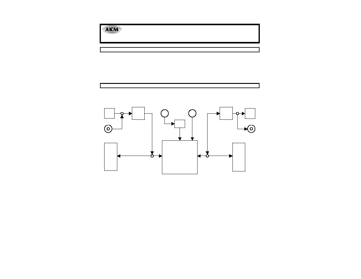
The AKD4125-A is an evaluation board for AK4125, the digital sample rate converter. The AKD4125-A
has the digital audio interface and can achieve the interface with digital audio system via opt-connector.
Ordering guide
AKD4125-A --- AK4125 Evaluation Board
FUNCTION
∑
DIR/DIT with optical input/output
∑
10pin Header for AKM AD/DA evaluation board
Opt In
AK4114
10pin
Header
DSP
Data
5V
GND
Opt Out
AK4114
10pin
Header
DSP
Data
AK4125
COAX
Regulator
COAX
Figure 1. AKD4125-A Block Diagram
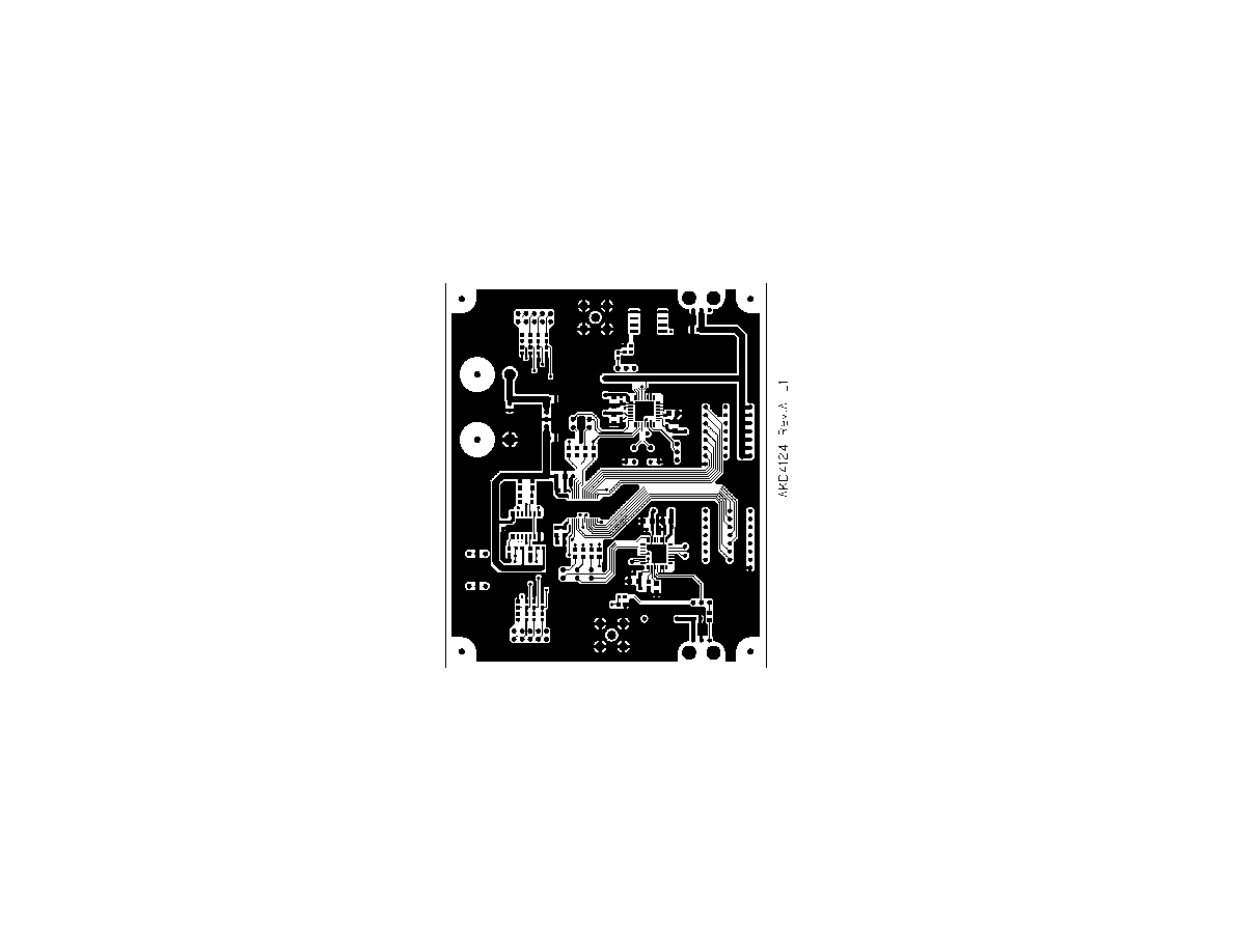
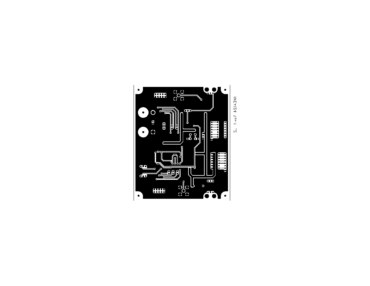
* Circuit diagram and PCB layout are attached at the end of this manual.
AK4125 Evaluation Board Rev.0
AKD4125-A
ASAHI KASEI
[AKD4125-A]
<KM078700>
2005/06
- 2 -
Operation sequence
1) Set up the power supply lines.
[VCC] (red)
=
+5V
(for
regulator)
[DGND] (black)
=
0V
Each supply line should be distributed from the power supply unit.
The regulator can be supplied 3.3V to all circuits.
2) Set up the evaluation mode, jumper pins. (See the followings.)
3) Power on.
The AK4125 should be reset once bringing SW1 (PDN) "L" upon power-up.
Evaluation mode
(1) Setting for Input port
(1) When using DIR function of AK4114 (U3)
When using PORT1 (DIR) or J1 (COAX), nothing should be connected to PORT2 (INPUT).
JP2
IBICK
JP3
SDTI
JP4
ILRCK
∑ SW3 setting (See Table 1)
Upper-side is "H" and lower-side is "L".
The audio interface format of the AK4114 is fixed to 24bit, MSB justified. IDIF2-0 and PLL2-0 of SW3
should be used by default setting.
SW3 No.
Name
ON ("H")
OFF ("L")
Default
1 DITH Dither
ON Dither
OFF L
2 PLL2
H
3 PLL1
L
4 PLL0
PLL Mode Setting
Fixed to default
H
5 IDIF0
L
6 IDIF1
H
7 IDIF2
AK4125 Audio I/F Format Setting
Fixed to default
L
Table 1. SW3 Setting

ASAHI KASEI
[AKD4125-A]
<KM078700>
2005/06
- 3 -
(2) All clocks are fed through the 10pin port
When using PORT2 (INPUT), nothing should be connected to J1 (COAX) and PORT1 (DIR).
JP2
IBICK
JP3
SDTI
JP4
ILRCK
∑ SW3 setting (See Table 2)
Upper-side is "H" and lower-side is "L".
SW3 No.
Name
ON ("H")
OFF ("L")
Default
1 DITH Dither
ON Dither
OFF L
2 PLL2
H
3 PLL1
L
4 PLL0
PLL Mode Setting
Refer to Table 3
H
5 IDIF0
L
6 IDIF1
H
7 IDIF2
AK4125 Audio I/F Format Setting
Refer to Table 4
L
Table 2. SW3 Setting
Mode Master
/
Slave PLL2 PLL1 PLL0
ILRCK
Freq IBICK
Freq IMCLK
SMUTE
(Note 4)
0 L
L
L
8k 96kHz
1 L
L
H
Manual
2 L
H
L
8k
216kHz
16k
216kHz
(Note 1)
Depending on
IDIF2-0
Not
needed.
Semi-Auto
3 L
H
H Reserved
4 H
L
L
32fsi
(Note
3)
5 H
L
H 64fsi
6 H
H
L 128fsi
Manual
7
Slave
IMCLK = DVSS
IBICK = Input
ILRCK = Input
H H H
8k
216kHz
(Note 2)
64fsi
Not
needed.
Semi-Auto
8 L
L
L
8k
216kHz
128fs
9 L
L
H
8k
108kHz
256fs
10 L
H
L
8k 54kHz
512fs
Manual
11 L
H
H
8k
216kHz
128fs Semi-Auto
12 H
L
L
8k
216kHz
192fs
13 H
L
H
8k 108kHz
384fs
14 H
H
L
8k
54kHz
768fs
Manual
15
Master
IMCLK = Input
IBICK = Output
ILRCK = Output
H H H
8k 216kHz
64fs
192fs Semi-Auto
Table 3. PLL Setting (Input PORT)
Note 1. PLL lock rage is changed by the value of R and C connected FILT pin. Refer to "PLL Loop Filter" in the
datasheet.
470, 0.22µF and 1nF are implemented on the evaluation board.
Note 2. The IBCIK must be continuous except when the clocks are changed.
Note 3. IBCIK = 32fsi is supported only 16bit LSB justified and I
2
S Compatible.
Note 4. Refer to "Soft Mute Operation" for Manual mode and Semi-Auto mode in the datasheet.

ASAHI KASEI
[AKD4125-A]
<KM078700>
2005/06
- 4 -
Mode IDIF2 IDIF1 IDIF0
SDTI Format
ILRCK
IBICK
IBICK Freq
Master / Slave
0 L L L 16bit,
LSB
justified
32fsi
1
L
L
H
20bit, LSB justified
40fsi
2 L H L 24/20bit,
MSB
justified
48fsi
3 L H H
24/16bit,
I
2
S Compatible
48fsi or
32fsi
4
H
L
L
24bit, LSB justified
Input Input
48fsi
Slave
5 H L H 24bit,
MSB
justified
64fs
6 H H L 24bit,
I
2
S Compatible
Output
Output
64fs
Master
7 H H H
Reserved
Table 4. Input Audio Interface Format (Input PORT)
(2) Setting for Output port
(1) When using DIT function of AK4114 (U4)
When using PORT4 (DIT) or J2 (TX), nothing should be connected to PORT3 (OUTPUT). When BICK and
LRCK frequencies are changed, the value of X'tal (X1) frequency should be changed.
JP6
OBICK
JP7
OLRCK
∑ SW4 setting (See Table 5)
Upper-side is "H" and lower-side is "L".
The audio interface format of the AK4114 is fixed to 24bit, MSB justified. ODIF2-0, CMODE2-0 and
OBIT1-0 of SW3 should be used by default setting.
SW4 No.
Name
ON ("H")
OFF ("L")
Default
1 ODIF1
H
2 ODIF0
AK4125 Output Audio I/F Format Setting
Fixed to default
L
3 CMODE2
H
4 CMODE1
L
5 CMODE0
AK4125 Mode Setting
Fixed to default
L
6 OBIT1
H
7 OBIT0
AK4125 Output bit Length Setting
Fixed to default
H
Table 5. SW4 Setting

ASAHI KASEI
[AKD4125-A]
<KM078700>
2005/06
- 5 -
(2) All clocks are fed through the 10pin port
When using PORT3 (OUTPUT), nothing should be connected to J2 (TX) and PORT4 (DIT).
JP6
OBICK
JP7
OLRCK
∑ SW4 setting (See Table 6)
Upper-side is "H" and lower-side is "L".
SW4 No.
Name
ON ("H")
OFF ("L")
Default
1 ODIF1
H
2 ODIF0
AK4125 Output Audio I/F Format Setting
Refer to Table 7
L
3 CMODE2
H
4 CMODE1
L
5 CMODE0
AK4125 Mode Setting
Refer to Table 8
L
6 OBIT1
H
7 OBIT0
AK4125 Output bit Length Setting
Refer to Table 9
H
Table 6. SW4 Setting
Mode ODIF1 ODIF0 SDTO
Format
0 L L LSB
justified
1 L H (Reserved)
2 H L MSB
justified
3 H H
I
2
S Compatible
Table 7. Output Audio Interface Format 1 (Output PORT)
Mode CMODE2 CMODE1 CMODE0
Master
/
Slave
OMCLK
fso
0 L L L Master
256fso 8k
108kHz
1 L L H Master
384fso 8k
108kHz
2 L H L Master
512fso
8k 54kHz
3 L H H Master
768fso
8k
54kHz
4
H
L
L
Slave
Not used. Set to DVSS.
8k
216kHz
5 H L H Master
128fso 8k
216kHz
6 H H L Master
192fso 8k
216kHz
7
H
H
H
Master (Bypass)
Not used. Set to DVSS.
8k 216kHz
Table 8. Master/Slave Control (Output PORT)
Mode OBIT1 OBIT0 SDTO
Output
0 L L 16bit
1 L H 18bit
2 H L 20bit
3 H H 24bit
Table 9. Output Audio Interface Format 2 (Output PORT)

ASAHI KASEI
[AKD4125-A]
<KM078700>
2005/06
- 6 -
Other jumper pins set up
1. JP1 (RX) : Select of RX input
COAX: COAX input.
RX: Optical
input.
<Default>
2. JP5 (CKSO) : AK4114 BICK and LRCK setting
H: BICK: 2.048MHz
12.288MHz, LRCK: 32kHz 192kHz
L: BICK: 2.048MHz
6.144MHz, LRCK: 32kHz 96kHz <Default>
When BICK and LRCK frequencies are changed, the value of X'tal (X1) frequency should be changed.
3. JP8 (TX) : Select of TX output
BNC: BNC connector (J2) output.
OPT: Optical (PORT4) output. <Default>
The function of the toggle SW
Upper-side is "H" and lower-side is "L".
[SW1] (PDN): Resets the AK4125 and the AK4114. Keep "H" during normal operation.
The AK4125 and the AK4114 should be resets once bringing "L" upon power-up.
[SW2] (SMUTE): Soft mute of AK4125
Indication for LED
[LED1] (UNLOCK): Monitor UNLOCK pin of the AK4125. LED turns on when unlock occurs.
[LED2] (ERF): Monitor INT0 pin of the AK4114 (U3). LED turns on when unlock or parity error occurs.

ASAHI KASEI
[AKD4125-A]
<KM078700>
2005/06
- 7 -
MEASUREMENT RESULTS
[Measurement condition]
∑ Measurement unit : Audio Precision, System Two Cascade
∑ Power Supply : AVDD = DVDD = 3.3V
∑
Band
width
:
10Hz
FSO/2
∑
Temperature :
Room
[Measurement Result]
SRC Characteristics
Result
Unit
THD+N (Input = 1kHz, 0dBFS)
FSO/FSI = 44.1kHz/48kHz
FSO/FSI = 48kHz/44.1kHz
FSO/FSI = 48kHz/192kHz
FSO/FSI = 192kHz/48kHz
Worst Case (FSO/FSI = 44.1kHz/8kHz)
130.2
124.9
130.6
124.3
116.7
dB
dB
dB
dB
dB
Dynamic Range (Input = 1kHz,
-60dBFS)
FSO/FSI = 44.1kHz/48kHz
FSO/FSI = 48kHz/44.1kHz
FSO/FSI = 48kHz/192kHz
FSO/FSI = 192kHz/48kHz
Worst Case (FSO/FSI = 192kHz/192kHz)
Dynamic Range (Input = 1kHz,
-60dBFS, A-weighted)
FSO/FSI = 44.1kHz/48kHz
136.2
136.4
136.1
132.3
132.2
139.6
dB
dB
dB
dB
dB
dB

ASAHI KASEI
[AKD4125-A]
<KM078700>
2005/06
- 8 -
[Plot]
AK4125 THD+N vs Input Level (fsi=48KHz,fso=44.1KHz) AVDD=DVDD=3.3V,fin=1KHz
-120
+0
-110
-100
-90
-80
-70
-60
-50
-40
-30
-20
-10
dBFS
-150
-120
-148
-146
-144
-142
-140
-138
-136
-134
-132
-130
-128
-126
-124
-122
d
B
F
S
Fig 1. THD+N vs. Input Level
AK4125 THD+N vs Input Frequency (fsi=48KHz,fso=44.1KHz) AVDD=DVDD=3.3V,Input Level=0dBFS
20
20k
50
100
200
500
1k
2k
5k
10k
Hz
-150
-80
-145
-140
-135
-130
-125
-120
-115
-110
-105
-100
-95
-90
-85
d
B
F
S
Fig 2. THD+N vs. Input Frequency (Input = 0dBFS)

ASAHI KASEI
[AKD4125-A]
<KM078700>
2005/06
- 9 -
AK4125 THD+N vs Input Frequency (fsi=48KHz,fso=44.1KHz) AVDD=DVDD=3.3V,Input Level=-60dBFS
20
20k
50
100
200
500
1k
2k
5k
10k
Hz
-180
-100
-175
-170
-165
-160
-155
-150
-145
-140
-135
-130
-125
-120
-115
-110
-105
d
B
F
S
Fig 3. THD+N vs. Input Frequency (Input =
-60dBFS)
AK4125 Linearity (fsi=48KHz,fso=44.1KHz) AVDD=DVDD=3.3V,fin=1KHz
-150
+0
-140
-130
-120
-110
-100
-90
-80
-70
-60
-50
-40
-30
-20
-10
dBFS
-150
+0
-140
-130
-120
-110
-100
-90
-80
-70
-60
-50
-40
-30
-20
-10
d
B
F
S
Fig 4. Linearity
ASAHI KASEI
[AKD4125-A]
<KM078700>
2005/06
- 10 -
AK4125 Frequency_Response (fsi=48KHz,fso=44.1KHz) AVDD=DVDD=3.3V,Input=0dBFS
2k
22k
4k
6k
8k
10k
12k
14k
16k
18k
20k
Hz
-6
+1
-5.5
-5
-4.5
-4
-3.5
-3
-2.5
-2
-1.5
-1
-0.5
-0
+0.5
d
B
F
S
Fig 5. Frequency Response
AK4125 FFT Plot (fsi=48KHz,fso=44.1KHz) AVDD=DVDD=3.3V,Input=0dBFS,fin=1KHz
-200
+0
-190
-180
-170
-160
-150
-140
-130
-120
-110
-100
-90
-80
-70
-60
-50
-40
-30
-20
-10
d
B
F
S
20
20k
50
100
200
500
1k
2k
5k
10k
Hz
Fig 6. FFT Plot (Input = 0dBFS)
ASAHI KASEI
[AKD4125-A]
<KM078700>
2005/06
- 11 -
AK4125 FFT Plot (fsi=48KHz,fso=44.1KHz) AVDD=DVDD=3.3V,Input=-60dBFS,fin=1KHz
-200
+0
-190
-180
-170
-160
-150
-140
-130
-120
-110
-100
-90
-80
-70
-60
-50
-40
-30
-20
-10
d
B
F
S
20
20k
50
100
200
500
1k
2k
5k
10k
Hz
Fig 7. FFT Plot (Input = -60dBFS)
AK4125 Frequency_Response (Blue:fsi=48KHz, Red:fsi=96KHz, Green:fsi=192KHz) AVDD=DVDD=3.3V,fso=48KHz
2k
22k
4k
6k
8k
10k
12k
14k
16k
18k
20k
Hz
-8
+1
-7.5
-7
-6.5
-6
-5.5
-5
-4.5
-4
-3.5
-3
-2.5
-2
-1.5
-1
-0.5
-0
+0.5
d
B
F
S
Fig 8. Frequency Response
fsi=192kHz
fsi=96kHz
fsi=48kHz

ASAHI KASEI
[AKD4125-A]
<KM078700>
2005/06
- 12 -
AK4125 Frequency_Response (Yellow:fsi=44.1KHz, Blue:fsi=48KHz, Red:fsi=96KHz,Green:fsi=192KHz)
AVDD=DVDD=3.3V,fso=44.1KHz
2k
22k
4k
6k
8k
10k
12k
14k
16k
18k
20k
Hz
-8
+1
-7.5
-7
-6.5
-6
-5.5
-5
-4.5
-4
-3.5
-3
-2.5
-2
-1.5
-1
-0.5
-0
+0.5
d
B
F
S
Fig 9. Frequency Response
fsi=192kHz
fsi=96kHz
fsi=48kHz
fsi=44.1kHz
ASAHI KASEI
[AKD4125-A]
<KM078700>
2005/06
- 13 -
Revision History
IMPORTANT NOTICE
∑
These products and their specifications are subject to change without notice. Before considering any use
or application, consult the Asahi Kasei Microsystems Co., Ltd. (AKM) sales office or authorized distributor
concerning their current status.
∑
AKM assumes no liability for infringement of any patent, intellectual property, or other right in the application
or use of any information contained herein.
∑
Any export of these products, or devices or systems containing them, may require an export license or other
official approval under the law and regulations of the country of export pertaining to customs and tariffs,
currency exchange, or strategic materials.
∑
AKM products are neither intended nor authorized for use as critical components in any safety, life support,
or other hazard related device or system, and AKM assumes no responsibility relating to any such use,
except with the express written consent of the Representative Director of AKM. As used here:
(a) A hazard related device or system is one designed or intended for life support or maintenance of safety
or for applications in medicine, aerospace, nuclear energy, or other fields, in which its failure to function
or perform may reasonably be expected to result in loss of life or in significant injury or damage to
person or property.
(b) A critical component is one whose failure to function or perform may reasonably be expected to result,
whether directly or indirectly, in the loss of the safety or effectiveness of the device or system containing
it, and which must therefore meet very high standards of performance and reliability.
∑
It is the responsibility of the buyer or distributor of an AKM product who distributes, disposes of, or
otherwise places the product with a third party to notify that party in advance of the above content and
conditions, and the buyer or distributor agrees to assume any and all responsibility and liability for and hold
AKM harmless from any and all claims arising from the use of said product in the absence of such
notification.
Date
(YY/MM/DD)
Manual
Revision
Board
Revision
Reason Contents
05/06/30 KM078700 0
First Edition

A
A
B
B
C
C
D
D
E
E
E
E
D
D
C
C
B
B
A
A
VCC
ILRCK
IBICK
REG
SDTI
REG
IMCLK
OMCLK
REG
SDTO
OLRCK
OBICK
REG
REG
PDN
REG
REG
Title
Size
Document Number
Rev
Date:
Sheet
of
AK4125
0
AKD4125-A
A3
1
3
Monday, May 23, 2005
Title
Size
Document Number
Rev
Date:
Sheet
of
AK4125
0
AKD4125-A
A3
1
3
Monday, May 23, 2005
Title
Size
Document Number
Rev
Date:
Sheet
of
AK4125
0
AKD4125-A
A3
1
3
Monday, May 23, 2005
IDIF2
DITH
PLL1
IDIF1
IDIF0
PLL0
PLL2
ODIF1
OBIT0
ODIF0
CMODE2
CMODE1
OBIT1
CMODE0
H
H
L
L
For 74HC14 x 1
PDN
SMUTE
47K
DSS107
DSS107
47K
UNLOCK
INPUT
OUTPUT
2
1
3
SW1
ATE1D-2M3
SW1
ATE1D-2M3
C7
0.22u
C7
0.22u
R8
51
R8
51
C1
0.1u
C1
0.1u
C2
0.1u
C2
0.1u
2
1
D2
HSU119
D2
HSU119
9
8
U1D
74HC14
U1D
74HC14
C10
0.1u
C10
0.1u
R9
51
R9
51
1
2
U1A
74HC14
U1A
74HC14
11
10
U1E
74HC14
U1E
74HC14
C8
0.1u
C8
0.1u
C11
0.1u
C11
0.1u
R12
1k
R12
1k
R7
51
R7
51
FILT
1
AVSS
2
PDN
3
SMUTE
4
DITHER
5
PLL2
6
ILRCK
7
IBICK
8
SDTI
9
IDIF0
10
IDIF1
11
IDIF2
12
PLL0
13
PLL1
14
OBIT1
17
IMCLK
18
CMODE0
19
CMODE1
20
CMODE2
21
ODIF0
22
ODIF1
23
SDTO
24
OBICK
25
OLRCK
26
OMCLK
27
DVDD
28
DVSS
29
AVDD
30
UNLOCK
15
OBIT0
16
U2
AK4125
U2
AK4125
+
C4
47u
+
C4
47u
C5
1n
C5
1n
R6
51
R6
51
R1
10k
R1
10k
1
2
3
4
5
6
7
14
13
12
11
10
9
8
SW3
SW3
R11
51
R11
51
R2
470
R2
470
1
2
3
4
5
6
7
14
13
12
11
10
9
8
SW4
SW4
3
4
U1B
74HC14
U1B
74HC14
R10
51
R10
51
2
1
D1
HSU119
D1
HSU119
IN
OUT
GND
T1
TA48M33F
T1
TA48M33F
2
1
3
SW2
ATE1D-2M3
SW2
ATE1D-2M3
+
C9
10u
+
C9
10u
2
1
LED1
SML-210JT
LED1
SML-210JT
R3
10k
R3
10k
7
6
5
4
3
2
1
RP1
M8-1-473
RP1
M8-1-473
R4
51
R4
51
C3
0.1u
C3
0.1u
7
6
5
4
3
2
1
RP2
M8-1-473
RP2
M8-1-473
C6
0.1u
C6
0.1u
5
6
U1C
74HC14
U1C
74HC14
R5
51
R5
51

A
A
B
B
C
C
D
D
E
E
E
E
D
D
C
C
B
B
A
A
PDN
REG
IMCLK
IBICK
ILRCK
SDTI
Title
Size
Document Number
Rev
Date:
Sheet
of
INPUT
0
AKD4125-A
A3
2
3
Monday, May 23, 2005
Title
Size
Document Number
Rev
Date:
Sheet
of
INPUT
0
AKD4125-A
A3
2
3
Monday, May 23, 2005
Title
Size
Document Number
Rev
Date:
Sheet
of
INPUT
0
AKD4125-A
A3
2
3
Monday, May 23, 2005
ILRCK
IMCLK
IBICK
SDTI
COAX
OPT
DIF2 DIF1 DIF0
H
L
L
24bit, MSB justified
Setting
OCKS1
Setting
OCKS0
H
H
128fs, 192kHz
Setting
L
CM0
L
PLL=ON, RX Mode
CM1
RX(COAX)
RX(OPT)
INPUT
IBICK
SDTI
ILRCK
RX
ERF
R16
1k
R16
1k
+
C20
10u
+
C20
10u
R22
220k
R22
220k
R23
220k
R23
220k
C18
0.1u
C18
0.1u
R13
75
R13
75
R20
100
R20
100
C12
0.1u
C12
0.1u
JP3 HIF3G-50P-2.54DSA (2x1)
JP3 HIF3G-50P-2.54DSA (2x1)
C17
0.1u
C17
0.1u
1
2
3
4
5
6
7
8
9
10
PORT2
A1-10PA-2.54DSA
PORT2
A1-10PA-2.54DSA
+
C19
10u
+
C19
10u
R17
100
R17
100
IPS0
1
NC
2
DIF0
3
TEST2
4
DIF1
5
NC
6
DIF2
7
IPS1
8
P/SN
9
XTL0
10
XTL1
11
TVDD
13
DVSS
14
TX0
15
TX1
16
BOUT
17
COUT
18
UOUT
19
VOUT
20
DVDD
21
DVSS
22
MCKO1
23
BICK
26
MCKO2
27
DAUX
28
XTO
29
XTI
30
PDN
31
CM0
32
CM1
33
OCKS1
34
OCKS0
35
INT0
36
AVDD
38
R
39
VCOM
40
AVSS
41
RX0
42
NC
43
RX1
44
TEST1
45
RX2
46
NC
47
RX3
48
VIN
12
LRCK
24
SDTO
25
INT1
37
U3
AK4114
U3
AK4114
L1
47u
L1
47u
2
1
LED2
SML-210JT
LED2
SML-210JT
C15
0.1u
C15
0.1u
JP4 HIF3G-50P-2.54DSA (2x1)
JP4 HIF3G-50P-2.54DSA (2x1)
C13
0.1u
C13
0.1u
13
12
U1F
74HC14
U1F
74HC14
JP1 HIF3G-50P-2.54DSA (3x1)
JP1 HIF3G-50P-2.54DSA (3x1)
OUT
1
VCC
3
GND
2
PORT1
TORX141
PORT1
TORX141
R18
100
R18
100
J1
BNC-R-PC
J1
BNC-R-PC
R21
220k
R21
220k
+
C16
0.47u
+
C16
0.47u
R15
18k
R15
18k
+
C14
10u
+
C14
10u
R19
100
R19
100
JP2 HIF3G-50P-2.54DSA (2x1)
JP2 HIF3G-50P-2.54DSA (2x1)
R14
470
R14
470
R24
220k
R24
220k

A
A
B
B
C
C
D
D
E
E
E
E
D
D
C
C
B
B
A
A
PDN
SDTO
OMCLK
OBICK
REG
OLRCK
Title
Size
Document Number
Rev
Date:
Sheet
of
OUTPUT
0
AKD4125-A
A3
3
3
Monday, May 23, 2005
Title
Size
Document Number
Rev
Date:
Sheet
of
OUTPUT
0
AKD4125-A
A3
3
3
Monday, May 23, 2005
Title
Size
Document Number
Rev
Date:
Sheet
of
OUTPUT
0
AKD4125-A
A3
3
3
Monday, May 23, 2005
SDTO
OLRCK
OBICK
OMCLK
OPT
BNC
L
DIF0
256fs, 96kHz
H
L
Setting
CM1
PLL=OFF, X'tal Mode
OCKS1
L
H
L
L
24bit, MSB justified
CM0
Setting
Setting
128fs, 192kHz
DIF2
H
H
OCKS0
DIF1
L
H
TX(OPT)
TX(BNC)
1:1
TX
CKSO
OBICK
OLRCK
OUTPUT
11.2896MHz
C22
0.1u
C22
0.1u
R25
100
R25
100
JP6 HIF3G-50P-2.54DSA (2x1)
JP6 HIF3G-50P-2.54DSA (2x1)
+
C29
10u
+
C29
10u
R34
150
R34
150
GND
1
VCC
2
IN
3
PORT4
TOTX141
PORT4
TOTX141
J2
BNC-R-PC
J2
BNC-R-PC
+
C21
10u
+
C21
10u
R32
220k
R32
220k
R27
100
R27
100
R26
100
R26
100
C31
0.1u
C31
0.1u
1
2
3
4
5
6
7
8
9
10
PORT3
A1-10PA-2.54DSA
PORT3
A1-10PA-2.54DSA
C26
0.1u
C26
0.1u
+
C23
0.47u
+
C23
0.47u
T2
DA-02F
T2
DA-02F
C24 (open)
C24 (open)
JP5 HIF3G-50P-2.54DSA (3x1)
JP5 HIF3G-50P-2.54DSA (3x1)
JP8 HIF3G-50P-2.54DSA (3x1)
JP8 HIF3G-50P-2.54DSA (3x1)
C27
0.1u
C27
0.1u
C30
0.1u
C30
0.1u
R31
220k
R31
220k
IPS0
1
NC
2
DIF0
3
TEST2
4
DIF1
5
NC
6
DIF2
7
IPS1
8
P/SN
9
XTL0
10
XTL1
11
TVDD
13
DVSS
14
TX0
15
TX1
16
BOUT
17
COUT
18
UOUT
19
VOUT
20
DVDD
21
DVSS
22
MCKO1
23
BICK
26
MCKO2
27
DAUX
28
XTO
29
XTI
30
PDN
31
CM0
32
CM1
33
OCKS1
34
OCKS0
35
INT0
36
AVDD
38
R
39
VCOM
40
AVSS
41
RX0
42
NC
43
RX1
44
TEST1
45
RX2
46
NC
47
RX3
48
VIN
12
LRCK
24
SDTO
25
INT1
37
U4
AK4114
U4
AK4114
R29
220k
R29
220k
C25
(open)
C25
(open)
R33
240
R33
240
R30
220k
R30
220k
JP7 HIF3G-50P-2.54DSA (2x1)
JP7 HIF3G-50P-2.54DSA (2x1)
R28
100
R28
100
1
2
X1 HC-49/U
X1 HC-49/U
+
C28
10u
+
C28
10u