
ASAHI KASEI
[AKD4121]
<KM069301>
2004/08
- 1 -
GENERAL DESCRIPTION
The AKD4121 is the evaluation board for the AK4121, 96kHz asynchronous sample rate converter. This
board has the optical connectors to interface with other digital audio equipments and serial interfaces for
AKM AD/DA evaluation boards. The AKD4121 achieves quick evaluation of AK4121
Ordering guide
AKD4121 --- Evaluation board for AK4121
FUNCTION
Optical fiber connectors (for Digital Audio Interface. input x 1, output x 1.)
10pin Header (for AKM AD/DA evaluation board. input x 1, output x 1.)
On board X'tal Oscillator (input x 1, output x 1.)
10pin Header
(AK4112B)
DIR
AK4121
(AK4114)
Clock
Generator
3
JP1
IMCLK
JP2 4
PDN
SW1
SMUTE
SW2
3
3
IMCLK
IBICK
ILRCK
SDTI
3
DIR
JP6
DIT-SOURCE
JP11
3
Bypass
SRC-MCLK
JP5
PORT3
PORT1
OMCLK
OBICK
SDTO
OLRCK
D5V
+3.3V
+3.3V
D5V
D5V
+3.3V
DIT
Optical
Input
PORT2
~
+3.3V
D5V
T1
48M003F
OUT
GN
D
IN
5V or 3.3V
3
Optical
Output
PORT4
SW3
fsi-DIR
SW4
CMODE
SW5
fso
2
3
2
3
JP7~9
10pin Header
IN
OUT
PORT3
PORT3
DIT
JP10
3.3V
REG
JACK
Figure 1. AKD4121 Block Diagram
*Circuit diagram and PCB layout are attached at the end of this manual.
AK4121 Evalation Board Rev.B
AKD4121

ASAHI KASEI
[AKD4121]
<KM069301>
2004/08
- 2 -
Evaluation Board Manual Contents
Operating Sequence
--------------------------------------------------------------------------------------- p. 3
1. Jumper Setting for Power Supply: JP10(REG)
2. Power Supply Line Setting
3. DIP switch and Jumper pin Setting
4. Power-on
DIP switch and Jumper pin Setting
------------------------------------------------------------------ p. 4
1. Setting of fsi (input fs) block -------------------------------------------------------------------------- p. 4
1-1. In case of using optical Input.
1-2. All clock are fed through the 10-pin port.
1-3. SDTI is fed through the 10-pin port and others are fed from the DIR(AK4112B).
2. Setting of fso (output fs) block ---------------------------------------------------------------------- p. 9
2-1. In case of providing clock from DIT.
2-2. In case of providing clock from 10pin PORT
2-2-1. AK4121 Master Mode.
2-2-2. AK4121 Slave Mode.
3. Bypass Mode --------------------------------------------------------------------------------------------------- p.22
4. Setting of the others -------------------------------------------------------------------------------------- p.22
4-1. De-emphasis filter.
4-2. Soft Mute.
Jumper List
--------------------------------------------------------------------------------------------------- p.21
DIP switch list
--------------------------------------------------------------------------------------------------- p.21
Toggle switch list
--------------------------------------------------------------------------------------------- p.22
LED
---------------------------------------------------------------------------------------------------------------- p.22
Mesurement Results
--------------------------------------------------------------------------------------- p.23
Important Notice
--------------------------------------------------------------------------------------------- p.28
Circuit diagram
PCB layout

ASAHI KASEI
[AKD4121]
<KM069301>
2004/08
- 3 -
Operating Sequence
Please use the AKD4121 according to the following sequence.
1. Jumper Setting for Power Supply: JP10(3.3V)
The JP10 (3.3V) selects power supply of the AKD4121.(3.3V or 5V.)
JACK : Providing power supply voltage with 3.3V. Opticlal input is not avaible.
REG : Providing power supply voltage with 5V. (3.3V is supplied via regulator on board.)
2.
Power Supply Line Setting
Each supply line should be distributed directly from the power supply unit with low impedance
connection.
5V or 3.3V : For power supply jack. 5V or 3.3V. (Power supply voltage is selectrd by JP10.)
GND : Groung
of
the
board.
0V.
3.
DIP Switch and Jumper Pins Setting (refer next page)
4.
Power-on
(After power is on, SW1 should be reset by setting "L"
"H" once.)
*
The reset is done by SW1 during opertion.
The AK4121 is powered down during SW1 is "L".The power down state is canceld by briging the SW1
to "H", at the same time, the AK4121 is reset.
ASAHI KASEI
[AKD4121]
<KM069301>
2004/08
- 4 -
DIP switch and Jumper pin setting
1. Setting of fsi (input fs) block
1-1. Optical input
(PORT2)
1-1-a. Jumper setting
Parts No.
Setting
JP1 (don't
care)
JP2 SHORT
JP3 SHORT
JP4 SHORT
SW3-4 OFF
X1 (don't
care)
Table 1. Jumper Setting (Refer following figures)
JP4
ILRCK
JP1
IMCLK
JP3
SDTI
JP2
IBICK
OUT
IN
Figure 2. Jumper Setting
1-1-b. Audio Interface Format setting(IIS only)
1 2 3 4 5
ID
IF
2
ID
IF1
ID
IF
0
SW3
fsi-DIR
DI
R
-
CM
0
1/2MCLK
MC
LK
Figure 3. DIP
switch
(SW3) setting

ASAHI KASEI
[AKD4121]
<KM069301>
2004/08
- 5 -
1-2. All clock are fed through the 10-pin port
1-2-a. Jumper setting
Parts No.
Setting
JP1 (don't
care)
JP2 OPEN
JP3 OPEN
JP4 OPEN
SW3-4 (don't
care)
X1
(don't care)
Table 2. Jumper Setting (Refer following figures)
JP4
ILRCK
JP1
IMCLK
JP3
SDTI
JP2
IBICK
OUT
IN
Figure 4. Jumper Setting
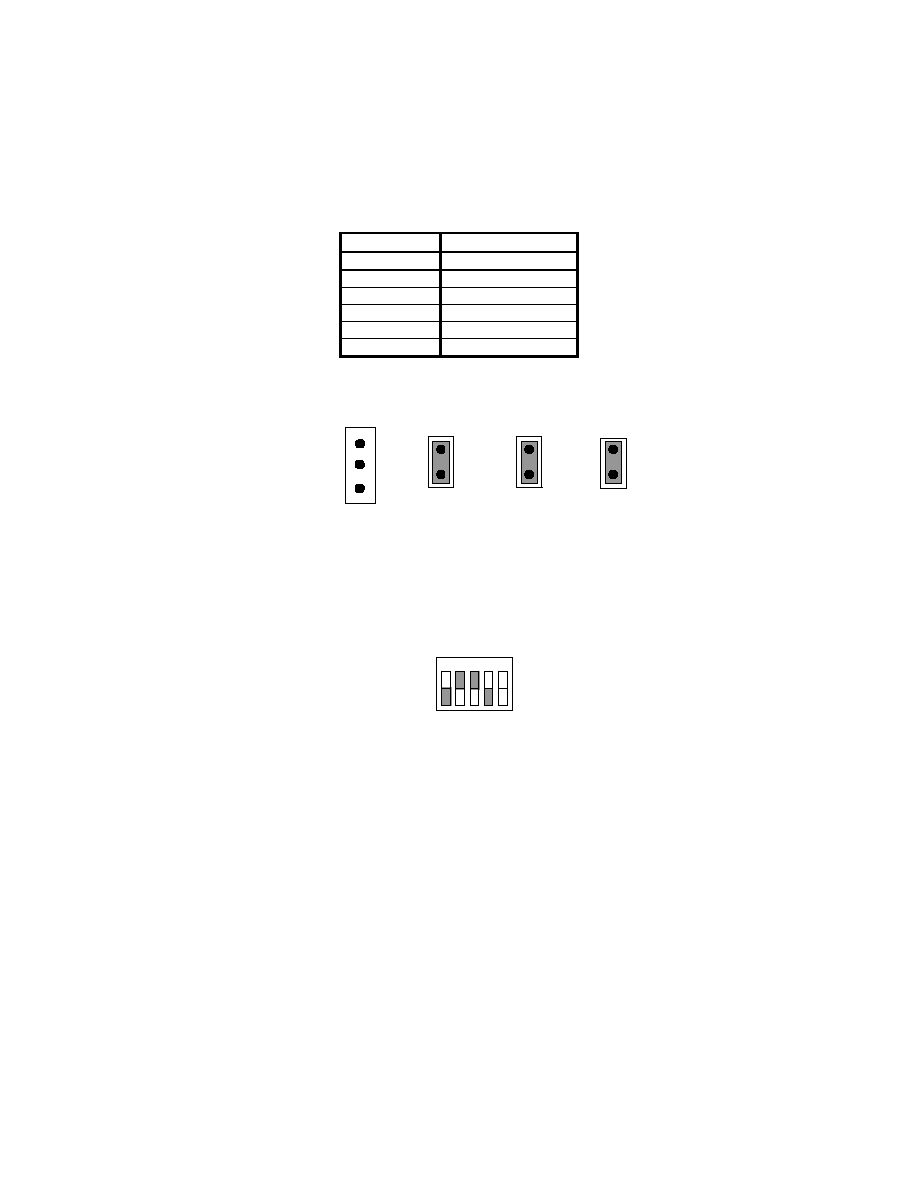
1-2-b. Audio Interface Format setting
SRC:AK4121
SW3-1 SW3-2 SW3-3
Audio Interface
Format
DIF2 DIF1 DIF0
16bit, Right justified
0 0 0
20bit, Right justified
0 0 1
Left justified
0 1 0
I
2
S
0 1 1
24bit, Right justified
1 0 0
Table 3. DIP
switch
(SW3) setting(Refer following figures)
1 2 3 4 5
ID
IF2
ID
IF1
ID
IF0
SW3
fsi-DIR
D
I
R-
CM
0
1/2MCLK
MC
L
K
1 2 3 4 5
ID
IF2
ID
IF1
ID
IF0
SW3
fsi-DIR
D
I
R-
CM
0
1/2MCLK
MC
L
K
16bit,
Right
justified 20bit,
Right
justified