 | –≠–ª–µ–∫—Ç—Ä–æ–Ω–Ω—ã–π –∫–æ–º–ø–æ–Ω–µ–Ω—Ç: AK9813B | –°–∫–∞—á–∞—Ç—å:  PDF PDF  ZIP ZIP |
ASAHI KASEI
[AK9813B]
DAD04E-01
2002/11
- 1 -
AK9813B
12ch 8bit D/A Converter with EEPROM
General Description
The AK9813B includes 12 channel, 8bit D/A converters with on-chip output buffer amps and it is
capable to store the input digital data of each DAC by on-chip non-volatile CMOS EEPROM. The
AK9813B is optimally designed for various circuit adjustments for consumer and industrial
equipments and it is ideally suited for replacing mechanical trimmers.
Features
EEPROM SECTION
12 words x 8bit x 4 organization for DAC
D/A CONVERTER SECTION
12 channels
Resolution : 8bit
DNL
: -1 to +2 LSB
INL
: ±1.5 LSB
Analog Output Voltage Range : GND to VCC
Operating Voltage Range
Digital section : 2.7V to 5.5V
Analog section : 4.5V to 5.5V, 2.7V to 3.6V
24pin VSOP
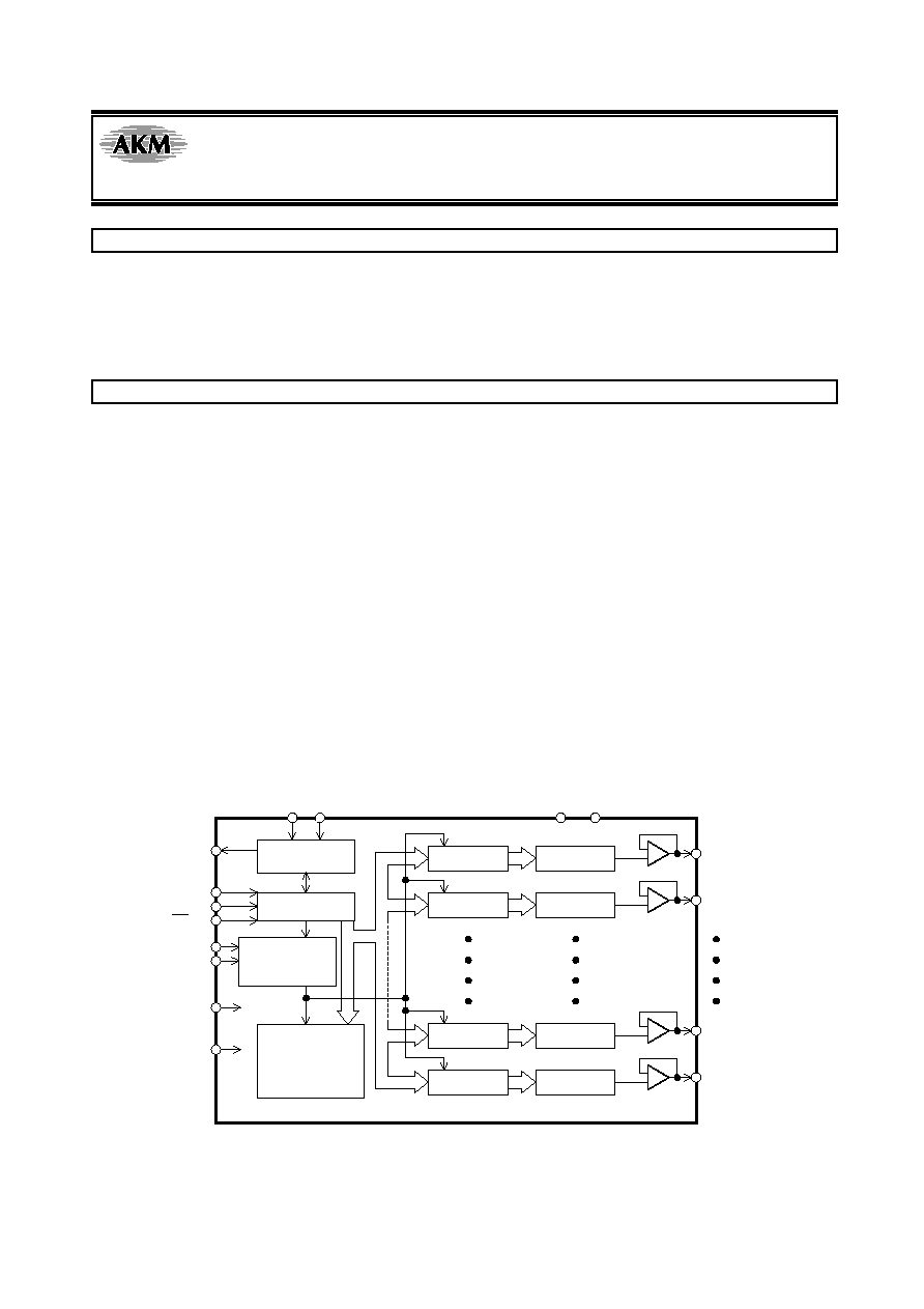
Block Diagram
Channel
& Address
Decoder
Shift
Register
8bit D/A
8bit D/A
8bit D/A
8bit Latch
8bit Latch
8bit Latch
EEPROM
384bit
(12 x 8bit x 4)
8
DI
CLK
DO
Control Logic
8
8bit Latch
+
--
8bit D/A
AO2
8
+
--
AO11
8
+
--
AO12
8
+
--
AO1
VDD
SEL
EA0
VCC
GND
CS/LD
ECL
EA1
VSS

ASAHI KASEI
[AK9813B]
DAD04E-01
2002/11
- 2 -
Ordering Guide
Model
Temp.
Range
Package
AK9813BF
-40 to +85∞C
24-pin VSOP
Pin Layout
17
16
15
14
13
12
11
10
VSS
GND
EA0
EA1
DI
CLK
DO
CS/LD
AO1
AO2
AO3
AO4
AO5
AO6
AO7
AO8
24
23
22
21
1
2
3
4
AK9813BF
20
19
18
5
6
7
8
ECL
SEL
VDD
VCC
AO9
AO10
AO11
AO12
9
24pin VSOP
ASAHI KASEI
[AK9813B]
DAD04E-01
2002/11
- 3 -
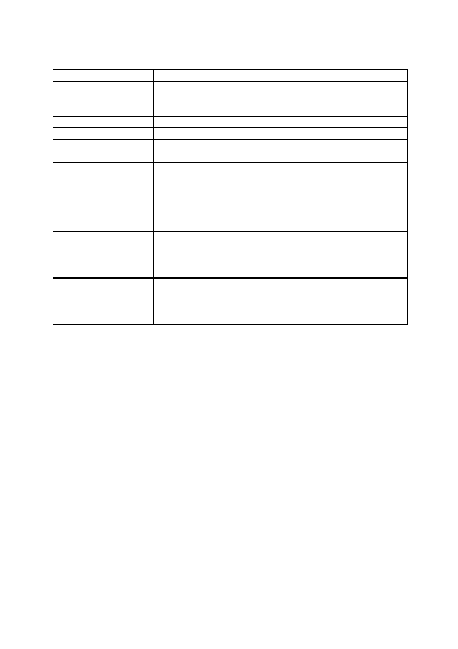
Pin Description (1)
No. Pin
Name I/O
Function
20
DI
I
Serial Data Input Pin
SEL=High : 16bit data input format
SEL=Low : 14bit data input format
17
DO
O
(SEL=High: CS I/F)
AK9813B reads out the data with LSB first in the 16bit shift
register to DO pin synchronously with falling edge of CLK.
When the CS pin is high level, the DO pin becomes high
impedance. In STATUS mode, the DO pin outputs Ready/Busy
status.
(SEL=Low: LD I/F)
AK9813B reads out the data with MSB first in the 14bit shift
register to DO pin synchronously with falling edge of CLK.
In WRITE mode, the DO pin outputs Ready/Busy status.
19
CLK
I
Shift Clock Input Pin (Schmitt-trigger input)
AK9813B takes in the data from DI pin synchronously with rising
edge of the CLK pin. The data are transferred to the internal
shift register.
18
CS/LD
I
Chip Select Input Pin (Schmitt-trigger input)
The CS/LD is internally pulled up to VCC.
(SEL=High: CS I/F)
After the CS pin changes from high level to low level while the
CLK pin is high level, the AK9813B can input the data to the
internal shift register and takes in the data from the DI pin
synchronously with the rising edge of the CLK pin.
After the CS pin changes from high level to low level while the
CLK pin is low level, the AK9813B becomes the status mode
and reads out the Ready/Busy status to the DO pin.
When the CS pin changes from low level to high level regardless
of Low/High level of the CLK pin, the AK9813B removes from
the status mode to the normal mode. The CS pin usually
should be kept at high level.
(SEL=Low: LD I/F)
When the LD pin receives high pulse, the data of the internal
shift register is transferred to the internal decoder or the register
for D/A. The LD pin usually should be kept at low level.
ASAHI KASEI
[AK9813B]
DAD04E-01
2002/11
- 4 -
Pin Description (2)
No. Pin
Name I/O
Function
1
12
AO1
AO12
O
8bit D/A outputs with OP-AMP
14 VCC
Digital section Power Supply Pin
23 GND
Digital section Ground Pin
13 VDD
OP-AMP and D/A section Power Supply
24 VSS
OP-AMP and D/A section Ground
21
22
EA0
EA1
I
(SEL=High: CS I/F)
In AUTO READ operation and ECL operation, the address of
EEPROM is selected by the EA0 and the EA1 pins.
(SEL=Low: LD I/F)
The address of EEPROM is selected by the EA0 and the EA1
pins.
16
ECL
I
When the ECL pin receives high pulse, the data in EEPROM is
automatically loaded to each corresponding D/A, starting from
AO1 to AO12 in order. Then each D/A output is settled to
pre-determined value.
15
SEL
I
Input Data Format Select Pin
SEL=High : CS I/F
SEL=Low : LD I/F
After power-up, this pin should be kept either at "high" or "Low."

ASAHI KASEI
[AK9813B]
DAD04E-01
2002/11
- 5 -
Data Configuration
AK9813B have a shift register in order to control the chip.
When the SEL pin is "H"(CS I/F), the shift register becomes 16bit configuration and the data on the
DI pin should be loaded with LSB first. When the SEL pin is "L"(LD I/F), the shift register becomes
14bit configuration and the data on the DI pin is loaded with MSB first.
The following description shows the configuration of the shift register.
The data set consist of 2-bits for the control of the internal EEPROM, 2-bits for the address of the
EEPROM (CS I/F only), 4-bits for select of D/A converter and 8-bits for the digital input data of the
8bit D/A converter and total data set is 16bits or 14bits.
Shift register configuration: SEL=High (CS I/F)
MSB
LSB
Last
First
A1 A0 CL WR D11 D10 D9 D8 D7 D6 D5 D4 D3 D2 D1 D0
EEPROM
ADDRESS
EEPROM
CONTROL
SELECTION FOR
D/A CONVERTER
DIGITAL INPUT DATA
FOR D/A CONVERTER
OUTPUT VOLTAGE FOR D/A CONVERTER
D7 D6 D5 D4 D3 D2 D1 D0
OUTPUT VOLTAGE
FOR D/A
A1 A0 EEPROM
ADDRESS
0 0 0 0 0 0 0 0 GND=VSS
0 0
ADDRESS:
0
0 0 0 0 0 0 0 1 VDD/255 x 1
0 1
ADDRESS:
1
0 0 0 0 0 0 1 0 VDD/255 x 2
1 0
ADDRESS:
2
1 1
ADDRESS:
3
1 1 1 1 1 1 1 0 VDD/255 x 254
1 1 1 1 1 1 1 1 VDD
D/A CONVERTER CHANNEL SELECTION
D11 D10 D9
D8
D/A CHANNEL
D11 D10 D9
D8
D/A CHANNEL
0 0 0 0 Don't
Care
1 0 0 0 AO8
0 0 0 1 AO1
1 0 0 1 AO9
0 0 1 0 AO2
1 0 1 0 AO10
0 0 1 1 AO3
1 0 1 1 AO11
0 1 0 0 AO4
1 1 0 0 AO12
0 1 0 1 AO5
1 1 0 1 Can't
use
0 1 1 0 AO6
1 1 1 0 Can't
use
0 1 1 1 AO7
1 1 1 1 Don't
Care
(NOTE) Above "Don't Care" state is valid only when AK9813B is in DAC mode or WRITE mode.
Refer to the following section "Instruction Set" about mode.

ASAHI KASEI
[AK9813B]
DAD04E-01
2002/11
- 6 -
Shift register configuration: SEL=Low (LD I/F)
LSB
MSB
Last
First
D0 D1 D2 D3 D4 D5 D6 D7 D8 D9 D10 D11 WR CL
DIGITAL INPUT DATA
FOR D/A CONVERTER
SELECTION FOR
D/A CONVERTER
EEPROM
CONTROL
OUTPUT VOLTAGE FOR D/A CONVERTER
D0 D1 D2 D3 D4 D5 D6 D7
OUTPUT VOLTAGE
FOR D/A
EA1 EA0 EEPROM
ADDRESS
0 0 0 0 0 0 0 0 GND=VSS
0 0
ADDRESS:
0
1 0 0 0 0 0 0 0 VDD/255 x 1
0 1
ADDRESS:
1
0 1 0 0 0 0 0 0 VDD/255 x 2
1 0
ADDRESS:
2
1 1
ADDRESS:
3
0 1 1 1 1 1 1 1 VDD/255 x 254
1 1 1 1 1 1 1 1 VDD
NOTE)
EEPROM ADDRESS is selected by
the EA0 and EA1 pins.
D/A CONVERTER CHANNEL SELECTION
D8 D9 D10 D11 D/A
CHANNEL
D8 D9 D10 D11 D/A
CHANNEL
0 0 0 0 Don't
Care
1 0 0 0 AO8
0 0 0 1 AO1
1 0 0 1 AO9
0 0 1 0 AO2
1 0 1 0 AO10
0 0 1 1 AO3
1 0 1 1 AO11
0 1 0 0 AO4
1 1 0 0 AO12
0 1 0 1 AO5
1 1 0 1 Can't
use
0 1 1 0 AO6
1 1 1 0 Can't
use
0 1 1 1 AO7
1 1 1 1 Don't
Care
(NOTE) Above "Don't Care" state is valid only when AK9813B is in DAC mode or WRITE mode.
Refer to the following section "Instruction Set" about mode.

ASAHI KASEI
[AK9813B]
DAD04E-01
2002/11
- 7 -
Instruction Set
The AK9813B can be controlled for the following mode. The following mode is common to the
LD I/F and the CS IF. When LD I/F is selected, "A1" and "A0" are set by the external pins (EA0 pin
and EA1 pin).
DAC mode (External DI pin -> D/A converter)
X Don't Care
A1 A0 CL WR D11 D10 D9 D8 D7 D6 D5 D4 D3 D2 D1 D0
Function
X X 0 0 D/A
CHANNEL
Digital
Data for D/A
D/A output
CALL mode (Internal EEPROM -> D/A converter)
X Don't Care
A1 A0 CL WR D11 D10 D9 D8 D7 D6 D5 D4 D3 D2 D1 D0
Function
ADDRESS
1 0 D/A
CHANNEL X X X X X X X X READ
The output of D/A converter is set by the data in the internal EEPROM.
ALL CALL mode (Internal EEPROM -> D/A converter)
X Don't Care
A1 A0 CL WR D11 D10 D9 D8 D7 D6 D5 D4 D3 D2 D1 D0
Function
ADDRESS
1 0 0 0 0 0 X X X X X X X X ALL
CHANNEL
READ
The outputs of all D/A converters are set by the data in the internal EEPROM.
...Internal ECL function
WRITE ENABLE mode (Internal EEPROM WRITE ENABLE)
X Don't Care
A1 A0 CL WR D11 D10 D9 D8 D7 D6 D5 D4 D3 D2 D1 D0
Function
X X 1 1 0 0 0 0 X X X X X X X X WRITE
ENABLE
After WRITE ENABLE mode is executed, the programming to the internal EEPROM is enabled.
Upon power-up and after the execution of the ECL function, the AK9813B is in the programming
disable state.
WRITE DISABLE mode (Internal EEPROM WRITE DISABLE)
X Don't Care
A1 A0 CL WR D11 D10 D9 D8 D7 D6 D5 D4 D3 D2 D1 D0
Function
X X 1 1 1 1 1 1 X X X X X X X X WRITE
DISABLE
After WRITE DISABLE mode is executed, the programming to the internal EEPROM is disabled.
WRITE mode (External DI pin -> Internal EEPROM)
X Don't Care
A1 A0 CL WR D11 D10 D9 D8 D7 D6 D5 D4 D3 D2 D1 D0
Function
ADDRESS
0
1
D/A CHANNEL
Digital Data for D/A
WRITE
The digital data for D/A (D0 to D7) is written into the specified address in the internal EEPROM.
The state of the internal EEPROM must be the programming enable state.
READ mode (Internal EEPROM -> External DO pin)
X Don't Care
A1 A0 CL WR D11 D10 D9 D8 D7 D6 D5 D4 D3 D2 D1 D0
Function
ADDRESS
1 1 D/A
CHANNEL X X X X X X X X EEPROM
DATA
output
The DO pin outputs the data in the internal EEPROM synchronously with the falling edge of the
input pulse of the CLK pin.
ASAHI KASEI
[AK9813B]
DAD04E-01
2002/11
- 8 -
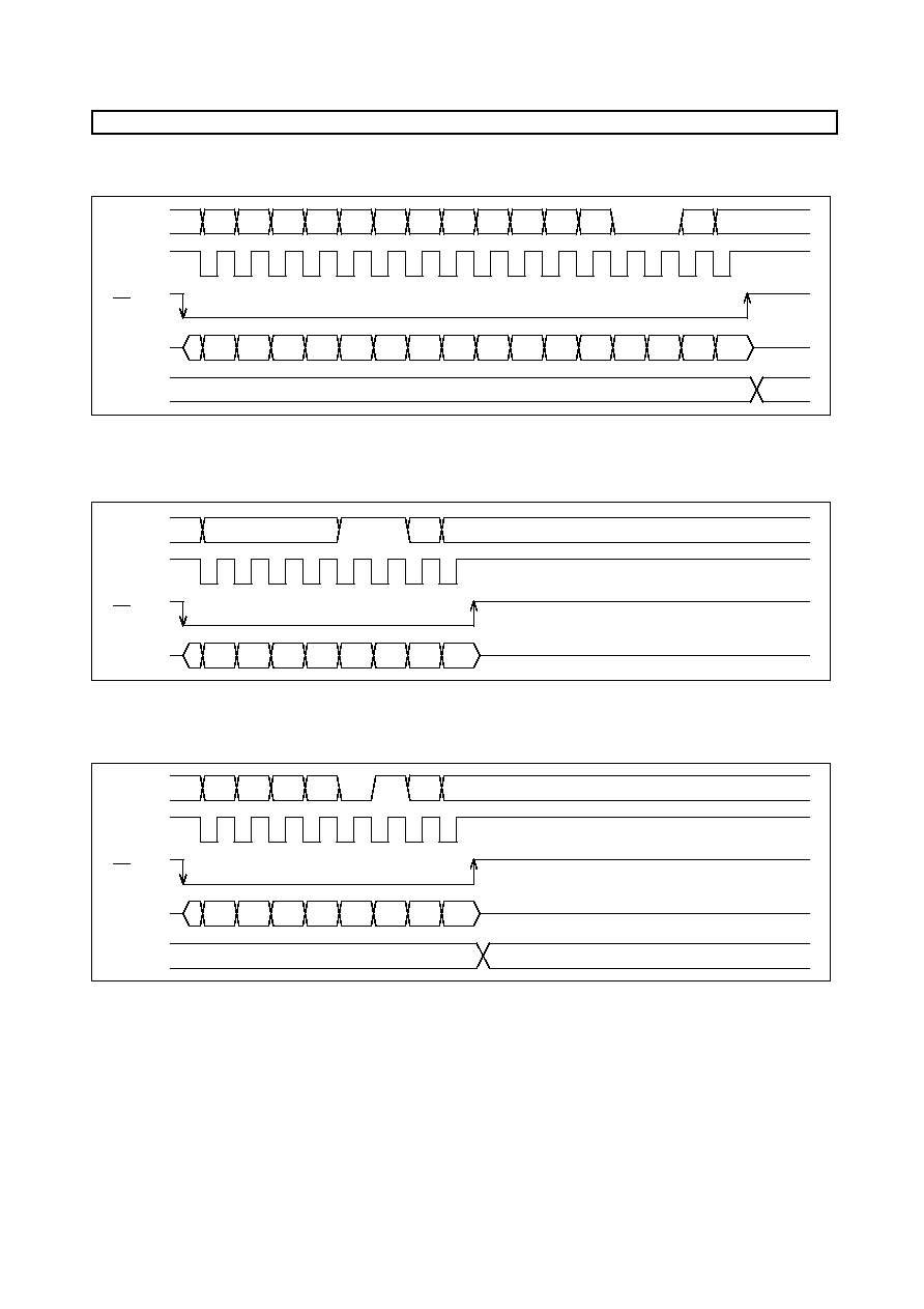
Functional Description
Timing Diagram for CS I/F (SEL="H")
1. DAC mode: The internal EEPROM is not used.
2. WRITE ENABLE/DISABLE mode: The programming state of the internal EEPROM is set.
3. CALL mode: The output of the D/A is set by the data in the internal EEPROM.
DI
CLK
CS/LD
DO
AO1 - 12
D0
D1
D2
D3
D4
D5
D6
D7
D8
D9
D10 D11 WR
CL
A0
A1
DI
CLK
CS/LD
DO
D8
D9
D10 D11 WR
CL
A0
A1
"1111"=WRITE DISABLE
"0000"=WRITE ENABLE
DI
CLK
CS/LD
DO
AO1 - 12
D8
D9
D10 D11 WR
CL
A0
A1
Output of selected channel changes.

ASAHI KASEI
[AK9813B]
DAD04E-01
2002/11
- 9 -
4. ALL CALL mode: The outputs of the all D/As are set by the data in the internal EEPROM.
∑The D/A outputs are set from AO1 to AO12 in order.
5. WRITE mode: The digital input data for D/A converter is written into the internal EEPROM.
6. READ mode: The data in the internal EEPROM is read from the DO pin.
DI
CLK
CS/LD
DO
AO1 - 12
D8
D9
D10 D11 WR
CL
A0
A1
DI
CLK
CS/LD
DO
AO1 - 12
D0
D1
D2
D3
D4
D5
D6
D7
D8
D9
D10 D11 WR
CL
A0
A1
No change
DI
CLK
CS/LD
DO
AO1 - 12
D0
D1
D2
D3
D8
D9
D10 D11 WR
CL
A0
A1
No change
Data for next mode or all "0"
D4
D5
D6
D7

ASAHI KASEI
[AK9813B]
DAD04E-01
2002/11
- 10 -
7. STATUS mode: The DO pin outputs the Ready/Busy status from the DO pin.
8. ECL function: For "H" pulse to the ECL pin, the data in the selected address in the internal
EEPROM is automatically loaded. Then each D/A converter output is settled to
pre-determined value.
9. Transfer mode for the cascade connection
In case that AK9813B devices are connected in cascade, the AK9813B under programming cycle
can transfer the data to the other AK9813B. The some AK9813B devices can be operated by
the common CS signal at the same time.
Please note that the input data into to the AK9813B under programming cycle should be all "0"
when the CS pin is changed from "L" to "H". If data except all "0" is input into the AK9813B
under programming cycle, accidental data disturbance may occur.
CLK
CS/LD
DO
AO1 - 12
Ready/Busy
No change
* : When the Ready/Busy is "L", it indicates the busy status. When AK9813B executes the CALL,
ALL CALL, READ, AUTOREAD or ECL operation, the DO pin outputs "L".
INVALID
EEPROM ADDRESS
EA0, EA1
ECL
AO1 - 12
*Analog output is set from AO1 to AO12 in order.
Output data to the next DAC
Data to the next DAC
DI
CLK
CS/LD
DO
AO1 - 12
CL
A0
A1
No operation
D0
D1
D2
D3
D4
D5
D6
D7
D8
D9 D10 D11 WR CL
A0
A1
D0
D1
D2
D3
D4
D5
D6
D7
D8
D9 D10 D11 WR CL
A0
A1

ASAHI KASEI
[AK9813B]
DAD04E-01
2002/11
- 11 -
Timing Diagram for LD I/F (SEL ="L")
1. DAC mode: The internal EEPROM is not used.
2. WRITE ENABLE/DISABLE mode: The programming state of internal EEPROM is set.
3. CALL mode: The output of the D/A is set by the data in the internal EEPROM.
D7
D8
D9
D10
D11
WR
CL
DI
CLK
CS/LD
DO
AO1 - 12
D0
D1
D2
D3
D4
D5
D6
DI
CLK
CS/LD
D11 D10
D9
D8
CL
WR
D7
"1111"=WRITE DISABLE
"0000"=WRITE ENABLE
D6
D5
D4
D3
D2
D1
D0
D7
D8
D9
D10
D11
WR
CL
DI
CLK
CS/LD
DO
AO1 - 12
D0
D1
D2
D3
D4
D5
D6
EA0, EA1

ASAHI KASEI
[AK9813B]
DAD04E-01
2002/11
- 12 -
4. ALL CALL mode: The outputs of the all D/As are set by the data in the internal EEPROM.
∑The D/A outputs are set from AO1 to AO12 in order.
5. WRITE mode: The digital input data for D/A converter is written into the internal EEPROM.
(NOTE)
* In case that AK9813B devices are connected in cascade, when a AK9813B device is under
programming cycle, the AK9813B device under programming cycle can not transfer the data to
the other AK9813B device and some AK9813B devices can not be operated by the common CS
signal at the same time.
* While programming cycle, the CS/LD pin should be "L".
* When the Ready/Busy signal from the DO pin is verified, the CS pin should be changed from "H"
to "L" and kept at "L". If the CS pin is kept at "H", the Ready/Busy signal does not output
correctly.
D7
D8
D9
D10
D11
WR
CL
DI
CLK
CS/LD
DO
AO1 - 12
D0
D1
D2
D3
D4
D5
D6
EA0, EA1
D7
D8
D9
D10
D11
WR
CL
DI
CLK
CS/LD
DO
AO1 - 12
D0
D1
D2
D3
D4
D5
D6
EA0, EA1
READY/BUSY
Output
No change

ASAHI KASEI
[AK9813B]
DAD04E-01
2002/11
- 13 -
6. READ mode: The data in the internal EEPROM is read from the DO pin.
7. ECL function:
When the ECL pin received high pulse, the data in EEPROM is automatically loaded to each
corresponding D/A, and starting from AO1 to AO12 in order. Then each D/A output is settled to
pre-determined value.
D0
D1
D7
D0
D7
D8
D9
D10
D11
WR
CL
DI
CLK
CS/LD
DO
AO1 - 12
D2
D3
D4
D5
D6
EA0, EA1
1
D1
7
8
9
10
11
12
13
14
Not change
Data for next mode or all "0"
INVALID DATA
(6bit)
VALID DATA (8bit: MSB first)
∑ ∑
∑ ∑
∑ ∑
∑ ∑
∑ ∑
∑ ∑
∑ ∑
∑ ∑
∑ ∑
∑ ∑
∑ ∑
∑ ∑
INVALID
EEPROM ADDRESS
EA0, EA1
ECL
AO1 - 12
* Analog outputs are set from AO1 to AO12 in order.

ASAHI KASEI
[AK9813B]
DAD04E-01
2002/11
- 14 -
Absolute Maximum Ratings
Parameter Symbol
Spec.
Unit
Power Supply
VCC
-0.6 to +7.0
V
Input Voltage
VIO
-0.6 to VCC+0.6
V
Ambient Temperature
Ta
-40 to +85
∞C
Storage Temperature
Tst
-65 to +150
∞C
Recommended Operating Conditions
Parameter Symbol Conditions Min
Typ
Max
Units
Power Supply 1
(Digital section)
VCC 2.7
5.5
V
VDD1 4.5
5.5
V
Power Supply 2
(DAC, AMP sections)
VDD2
2.7 3.6
V
Analog Output
Source Current 1
IAL
1
mA
Analog Output
Sink Current 1
IAH
VDD=4.5V to 5.5V
1
mA
Analog Output
Source Current 2
IAL
500
µA
Analog Output
Sink Current 2
IAH
VDD=2.7V to 3.6V
500
µA
Analog Output
Load Capacitance
AOC
1.0
µF

ASAHI KASEI
[AK9813B]
DAD04E-01
2002/11
- 15 -
Electrical Characteristics
DC Characteristics
(1) Digital Section
(VCC=2.7V to 5.5V, VDD=4.5V to 5.5V or 2.7V to 3.6V, GND, VSS=0V, Ta=-40∞C to +85∞C)
Parameter Symbol
Pin
Conditions Min Max
Units
Power Supply
(Digital Section)
VCC
2.7
5.5
V
Operating Current
(READ) (1)
(2)
ICC
VCC
CLK=1MHz
1.1
mA
Leakage Current
ILI
CLK, DI
CS/LD
EA0, EA1
ECL, SEL
VIN=VCC
-1.0
1.0
µA
High Level
Input Voltage 1
VIH
0.5xVCC
V
Low Level
Input Voltage 1
VIL
DI
EA0, EA1
ECL, SEL
0.2xVCC
V
High Level
Input Voltage 2
VIH
0.6xVCC
V
Low Level
Input Voltage 2
VIL
CS/LD
CLK
0.15xVCC
V
VOH1
4.5V
VCC5.5V
IOH=-400µA
VCC-0.4
V
High Level
Output Voltage
VOH2
DO
2.7V
VCC<4.5V
IOH=-200µA
0.7xVCC
V
VOL1
4.5V
VCC5.5V
IOH=1.0mA
0.4
V
Low Level
Output Voltage
VOL2
2.7V
VCC<4.5V
IOH=1.0mA
0.4
V
(1) All input pins are connected to either VCC or GND.
(2) DO=OPEN

ASAHI KASEI
[AK9813B]
DAD04E-01
2002/11
- 16 -
(2) Analog Section
(2-1) VDD=4.5V to 5.5V
(VCC=2.7V to 5.5V, VDD=4.5V to 5.5V, GND, VSS=0V, Ta=-40∞C to +85∞C)
Parameter Symbol
Pin
Conditions
Min
Typ
Max
Units
Power Supply 1
(Analog Section)
VDD1
4.5
5.0
5.5
V
Power Dissipation 1
(Analog Section)
IDD1
VDD
AOx=OPEN
7.0
mA
Resolution Res
8
bits
Integral (3)
Non-Linearity: INL
LE
-1.5
1.5
LSB
Differential
Non-Linearity: DNL
D
LE
AO1
AO12
AOx=OPEN
0.05V
AO
VDD-0.1V
-1.0
2.0
LSB
Buffer-AMP Minimum
Output Voltage 1
VAOL1
IAL=0µA
Data=00(Hex)
GND
0.05
V
Buffer-AMP Minimum
Output Voltage 2
VAOL2
IAL=500µA
Data=00(Hex)
-0.1
0.1
V
Buffer-AMP Minimum
Output Voltage 3
VAOL3
IAH=500µA
Data=00(Hex)
GND
0.1
V
Buffer-AMP Minimum
Output Voltage 4
VAOL4
IAL=1mA
Data=00(Hex)
-0.2
0.2
V
Buffer-AMP Minimum
Output Voltage 5
VAOL5
IAH=1mA
Data=00(Hex)
GND
0.2
V
Buffer-AMP Maximum
Output Voltage 1
VAOH1
IAH=0µA
Data=FF(Hex)
VDD-0.1
VDD
V
Buffer-AMP Maximum
Output Voltage 2
VAOH2
IAL=500µA
Data=FF(Hex)
VDD-0.2
VDD
V
Buffer-AMP Maximum
Output Voltage 3
VAOH3
IAH=500µA
Data=FF(Hex)
VDD-0.2
VDD+0.2
V
Buffer-AMP Maximum
Output Voltage 4
VAOH4
IAL=1mA
Data=FF(Hex)
VDD-0.3
VDD
V
Buffer-AMP Maximum
Output Voltage 5
VAOH5
AO1
AO12
IAH=1mA
Data=FF(Hex)
VDD-0.3
VDD+0.3
V
(3) Integral Non-Linearity is the error between the actual line and the ideal line. The
ideal line exhibits a perfect linear D/A converter output characteristic between the
input digital data"00" and the input digital data"FF".

ASAHI KASEI
[AK9813B]
DAD04E-01
2002/11
- 17 -
(2-2) VDD=2.7V to 3.6V
(VCC=2.7V to 3.6V, VDD=2.7V to 3.6V, GND, VSS=0V, Ta=-40∞C to +85∞C)
Parameter Symbol
Pin
Conditions
Min
Typ
Max
Units
Power Supply 2
(Analog Section)
VDD2
2.7
3.6
V
Power Dissipation 2
(Analog Section)
IDD2
VDD
AOx=OPEN
4.0
mA
Resolution Res
8
bits
Integral (4)
Non-Linearity: INL
LE
-1.5
1.5
LSB
Differential
Non-Linearity: DNL
D
LE
AOx=OPEN
0.15V
AO
VDD-0.15V
-1.0
2.0
LSB
Output Voltage for
Input Data "05"
0.1
0.15
V
Output Voltage for
Input Data "FA"
AO1
AO12 AOx=OPEN
VDD=3.3V
3.15
3.25
V
Buffer-AMP Minimum
Output Voltage 6
VAOL6
IAL=0µA
Data=00(Hex)
GND
0.05
V
Buffer-AMP Minimum
Output Voltage 7
VAOL7
IAL=250µA
Data=00(Hex)
-0.1
0.1
V
Buffer-AMP Minimum
Output Voltage 8
VAOL8
IAH=250µA
Data=00(Hex)
GND
0.1
V
Buffer-AMP Minimum
Output Voltage 9
VAOL9
IAL=500µA
Data=00(Hex)
-0.2
0.2
V
Buffer-AMP Minimum
Output Voltage 10
VAOL10
IAH=500µA
Data=00(Hex)
GND
0.2
V
Buffer-AMP Maximum
Output Voltage 6
VAOH6
IAH=0µA
Data=FF(Hex)
VDD-0.1
VDD
V
Buffer-AMP Maximum
Output Voltage 7
VAOH7
IAL=250µA
Data=FF(Hex)
VDD-0.2
VDD
V
Buffer-AMP Maximum
Output Voltage 8
VAOH8
IAH=250µA
Data=FF(Hex)
VDD-0.2
VDD+0.2
V
Buffer-AMP Maximum
Output Voltage 9
VAOH9
IAL=500µA
Data=FF(Hex)
VDD-0.3
VDD
V
Buffer-AMP Maximum
Output Voltage 10
VAOH10
AO1
AO12
IAH=500µA
Data=FF(Hex)
VDD-0.3
VDD+0.3
V
(4) Integral Non-Linearity is the error between the actual line and the ideal line. The
ideal line exhibits a perfect linear D/A converter output characteristic between the
input digital data"05" and the input digital data"FA".

ASAHI KASEI
[AK9813B]
DAD04E-01
2002/11
- 18 -
AC Characteristics
(1) CS I/F, LD I/F: Common Timing
(VCC=2.7V to 5.5V, VDD=4.5V to 5.5V or 2.7V to 3.6V, GND, VSS=0V, Ta=-40∞C to +85∞C)
Parameter Symbol
Conditions
Min
Max
Units
VCC Rise Time
tVCR
50
ms
Auto Address Hold Time
tVAH
3.5
ms
Auto Read Time
tPOR
Test Load 2
3.5
ms
tECW1 *1
100
ns
ECL "H" Pulse Width
tECW2 *2
250
ns
External Call Time
tECL
Test Load 2
3.5
ms
tESU1 *1
50
ns
Address Set Up Time
tESU2 *2
100
ns
ECL Address Hold Time
tEAH
3.5
ms
tECC1 *1
20
ns
Repeat Call Prohibition Time
tESCC2 *2
100
ns
*1: 4.5V
VCC5.5V
*2: 2.7V
VCC<4.5V
<AUTO READ>
<ECL FUNCTION>
90%
tVCR
10%
tVAH
tPOR
INVALID
(AC test measurement done at 90% and 10%points of VCC.)
(EA0/EA1 should be set at the same timing as VCC.)
VCC
EA0 / EA1
D/A Output(AO12)
tECW
tEAH
tECL
INVALID
ECL
EA0 / EA1
D/A Output
(AO12)
tESU
tECC

ASAHI KASEI
[AK9813B]
DAD04E-01
2002/11
- 19 -
(2) CS I/F Timing
(VCC=2.7V to 5.5V, VDD=4.5V to 5.5V or 2.7V to 3.6V, GND, VSS=0V, Ta=-40∞C to +85∞C)
Parameter Symbol Conditions Min
Max
Units
tCKL1
*5
200
ns
Clock "L" Pulse Width
tCKL2
*6
500
ns
tCKH1
*5
200
ns
Clock "H" Pulse Width
tCKH2
*6
500
ns
Clock Rising Time
Clock Falling Time
tCr
tCf
200
ns
tDSU1
*5
30
ns
Data Set Up Time
tDSU2
*6
150
ns
tDHD1
*5
60
ns
Data Hold Time
tDHD2
*6
150
ns
tCSU1
*5
100
ns
CS Set Up Time
tCSU2
*6
150
ns
CS Hold Time
tCCH
200
ns
DAC etc.
*3, *4, *5
100
ns
CS "H" Hold Time
tCSH
*3, *4, *6
250
ns
WRITE *4
7
ms
CALL, READ
15
µs
ALL CALL
3.5
ms
tDOD1
*5
200 ns
Data Output Enable Time
tDOD2
*6
500 ns
tDOZ1
*5
200 ns
Data Output Float Delay
tDOZ2
*6
500 ns
tDOC1
Test Load 1
*5
170
ns
Data Output Delay
tDOC2
*6
300 ns
DAC
Test Load 2
200
µs
D/A Output Setting Time
tCSD
CALL
Test Load 2
250
µs
ALL CALL
Test Load 2
3.5
ms
Status Set Up Time
tSSU
100
ns
tSHD1
*5
100
ns
Status Hold Time
tSHD2
*6
250
ns
*3: Please refer to "DAC etc" regarding CS "H" Hold Time before status mode execute.
*4: If READY/BUSY="H" is confirmed in status mode in the WRITE mode, the CS pin
can be changed to "L" shorter than the values specified on above.
Please refer to "DAC etc" regarding CS "H" Hold Time in case that AK9813B to be
connected in cascade is under programming cycle (READY/BUSY="L").
*5: 4.5V
VCC5.5V
*6: 2.7V
VCC<4.5V
ASAHI KASEI
[AK9813B]
DAD04E-01
2002/11
- 20 -
<Input / Output Waveform>
<STATUS Output>
90%
tCCH
tDOC
tDOC
tCKL
tCSD
CLK
DI
CS/LD
tDSU
tCKH
D/A Output
DO
10%
tCSH
tDHD
tCr
tCf
tDOZ
tCSU
tDOD
tSSU
tSHD
tDOD
(READY/BUSY STATUS)
CLK
CS/LD
DO
tDOZ
ASAHI KASEI
[AK9813B]
DAD04E-01
2002/11
- 21 -
(3) LD I/F Timing
(VCC=2.7V to 5.5V, VDD=4.5V to 5.5V or 2.7V to 3.6V, GND, VSS=0V, Ta=-40∞C to +85∞C)
Parameter Symbol Conditions Min
Max
Units
tCKL1
*5
200
ns
Clock "L" Pulse Width
tCKL2
*6
500
ns
tCKH1
*5
200
ns
Clock "H" Pulse Width
tCKH2
*6
500
ns
Clock Rising Time
Clock Falling Time
tCr
tCf
200
ns
tDCH1
*5
30
ns
Data Set Up Time
tDCH2
*6
150
ns
tCHD1
*5
60
ns
Data Hold Time
tCHD2
*6
150
ns
Load Set Up Time
tCHL
200
ns
tLDC1
*5
100
ns
Load Hold Time
tLDC2
*6
250
ns
tLDH1 modes
except
*5
100
ns
Load "H" Pulse Width
tLDH2 READ
mode
*6
250
ns
tLDH3
READ
mode
5
µs
tDO1
Test Load 1
*5
170
ns
Data Output Delay
tDO2
Test Load 1
*6
300
ns
DAC
Test Load 2
200
µs
D/A Output Setting Time
tLDD
CALL
Test Load 2
250
µs
ALL CALL
Test Load 2
3.5
ms
tASU1
*5
100
ns
Address Set Up Time
tASU2
*6
200
ns
tWAHD1
*5 20
ns
Write Address Hold Time
tWAHD2
*6 100
ns
Programming Cycle
tWRT
*7
7
ms
Ready Signal Delay
tRYD
Test Load 1
0.8
µs
tRYH1
Test Load 1
*5
20
ns
Repeat Write Prohibition
Time
tRYH2
Test Load 2
*6
100
ns
CALL, READ mode
15
µs
Read Hold Time
tRHD
ALL CALL mode
3.5
ms
CALL, READ mode
15
µs
Read Address Hold Time
tRAHD
ALL CALL mode
3.5
ms
*7: If READY/BUSY="L" is confirmed in status mode in the WRITE mode, the next
operation can be started.

ASAHI KASEI
[AK9813B]
DAD04E-01
2002/11
- 22 -
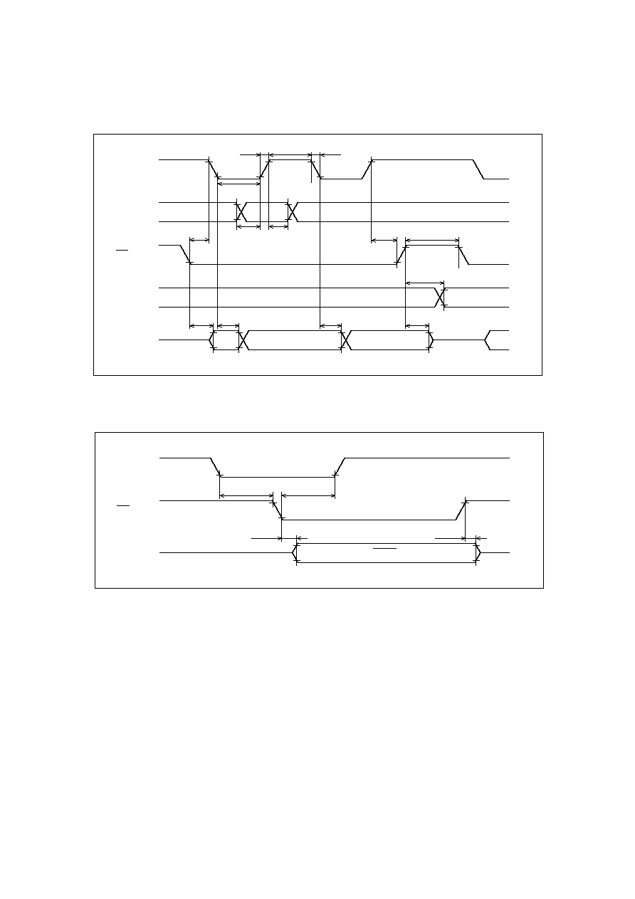
<Input / Output Waveform>
<Data Timing>
<WRITE mode>
* Please refer to the data timing regarding the input timing for the DI pin.
tRYD
tWRT
tASU
CLK
CS/LD
EA0 / EA1
READY/BUSY
STATUS
DO
tWAHD
tRYH
tCHL
tDO
tDO
tCKL
tLDD
CLK
DI
CS/LD
tDCH
tCKH
D/A Output
DO
90%
10%
tLDH
tCHD
tCr
tCf
tLDC
ASAHI KASEI
[AK9813B]
DAD04E-01
2002/11
- 23 -
<CALL mode>
<ALL CALL mode>
<READ mode>
* Please refer to the data timing regarding the input timing for the DI pin.
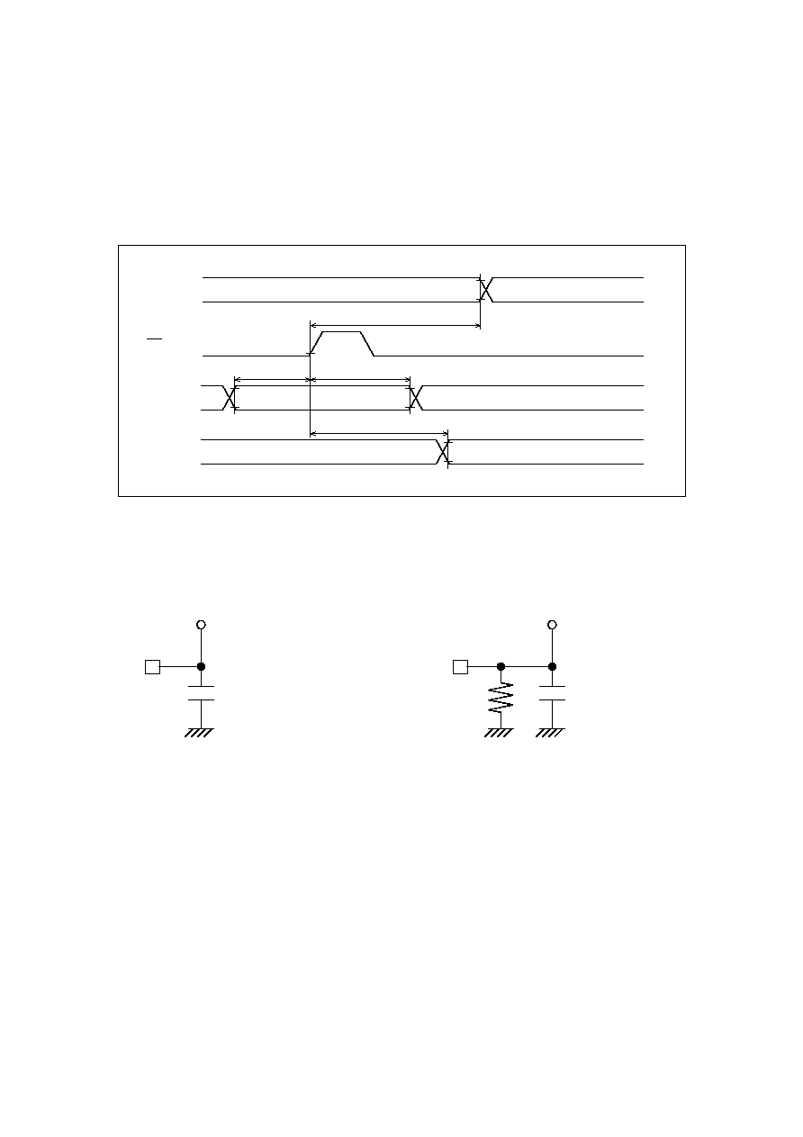
AC measurement circuit
Test
Load
1
Test Load 2
AC test point
Digital Input / Output Level : 50% / 20% of VCC
Analog Output Level
: 90% / 10% of VCC
Test Point
CL=20pF
~100pF
Test Point
CL=50pF
RAL=
10K
tRAHD
tRHD
tLDD
tASU
CLK
CS/LD
EA0 / EA1
D/A Output

IMPORTANT NOTICE
∑ These products and their specifications are subject to change without notice. Before considering any
use or application, consult the Asahi Kasei Microsystems Co., Ltd. (AKM) sales office or authorized
distributor concerning their current status.
∑ AKM assumes no liability for infringement of any patent, intellectual property, or other right in the
application or use of any information contained herein.
∑ Any export of these products, or devices or systems containing them, may require an export license
or other official approval under the law and regulations of the country of export pertaining to customs
and tariffs, currency exchange, or strategic materials.
∑ AKM products are neither intended nor authorized for use as critical components in any safety, life
support, or other hazard related device or system, and AKM assumes no responsibility relating to any
such use, except with the express written consent of the Representative Director of AKM. As used
here:
(a) A hazard related device or system is one designed or intended for life support or maintenance of
safety or for applications in medicine, aerospace, nuclear energy, or other fields, in which its
failure to function or perform may reasonably be expected to result in loss of life or in significant
injury or damage to person or property.
(b) A critical component is one whose failure to function or perform may reasonably be expected to
result, whether directly or indirectly, in the loss of the safety or effectiveness of the device or
system containing it, and which must therefore meet very high standards of performance and
reliability.
∑ It is the responsibility of the buyer or distributor of an AKM product who distributes, disposes of, or
otherwise places the product with a third party to notify that party in advance of the above content
and conditions, and the buyer or distributor agrees to assume any and all responsibility and liability
for and hold AKM harmless from any and all claims arising from the use of said product in the
absence of such notification.