 | –≠–ª–µ–∫—Ç—Ä–æ–Ω–Ω—ã–π –∫–æ–º–ø–æ–Ω–µ–Ω—Ç: AK5380 | –°–∫–∞—á–∞—Ç—å:  PDF PDF  ZIP ZIP |
ASAHI KASEI
[AK5380]
MS0100-E-00
2001/5
- 1 -
GENERAL DESCRIPTION
The AK5380 is a stereo A/D Converter with wide sampling rate of 4kHz
96kHz and is suitable for High-
end audio system. The AK5380 achieves high accuracy and low cost by using Enhanced dual bit
techniques. The AK5380 requires no external components because the analog inputs are single-ended.
The audio interface has two formats (MSB justified, I
2
S) and can correspond to many systems like music
instrument and AV receiver.
FEATURES
Stereo
ADC
On-Chip Digital Anti-Alias Filtering
Single-ended Input
Digital HPF for DC-Offset cancel
S/(N+D): 96dB@5V for 48kHz
DR:
106dB@5V for 48kHz
S/N:
106dB@5V for 48kHz
Sampling Rate Ranging from 4kHz to 96kHz
Master Clock:
256fs/384fs/512fs/768fs (
48kHz)
256fs/384fs
(
96kHz)
Input level: TTL/CMOS selectable
Output format: 24bit MSB justified / I
2
S selectable
Power Supply:
4.5
5.5V (VA)
2.7
5.5V (VD at 48kHz)
4.5
5.5V (VD at 96kHz)
Ta=-40
85
∞
C
Small 16pin TSSOP Package
AK5353 Pin-compatible
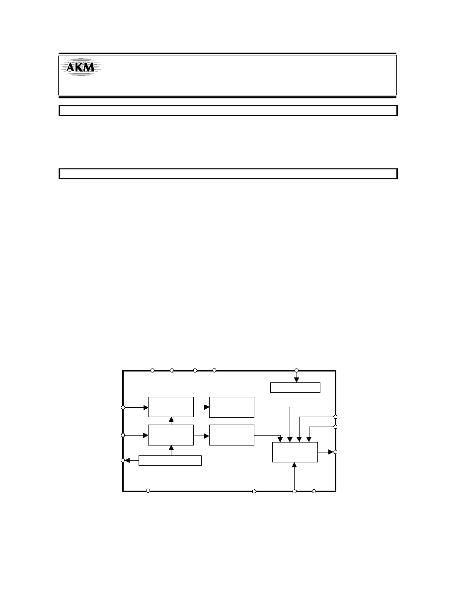
Modulator
MCLK
AINL
LRCK
SCLK
SDTO
DIF
VCOM
Clock Divider
AINR
AGND
VA
Decimation
Filter
Serial I/O
Interface
Voltage Reference
TTL
DGND
VD
TST
Modulator
Decimation
Filter
PDN
96kHz 24Bit
ADC with Single≠ended Input
AK5380

ASAHI KASEI
[AK5380]
MS0100-E-00
2001/5
- 2 -
Ordering Guide
AK5380VT
-40
+85
∞
C
16pin TSSOP
AKD5380
Evaluation Board
Pin Layout
1
AINR
AINL
VCOM
NC
AGND
VA
VD
DGND
Top
View
2
3
4
5
6
7
8
TST
TTL
PDN
DIF
SCLK
MCLK
LRCK
SDTO
16
15
14
13
12
11
10
9
The difference with AK5353
AK5353
AK5380
S/(N+D)
84dB
96dB
DR,S/N
96dB
106dB
VA(Analog Supply)
2.7 to 5.5V
4.5 to 5.5V
Input Resistance
60k
(@48kHz)
15k
(@48kHz)
Pin #3
VREF pin
NC pin
ASAHI KASEI
[AK5380]
MS0100-E-00
2001/5
- 3 -
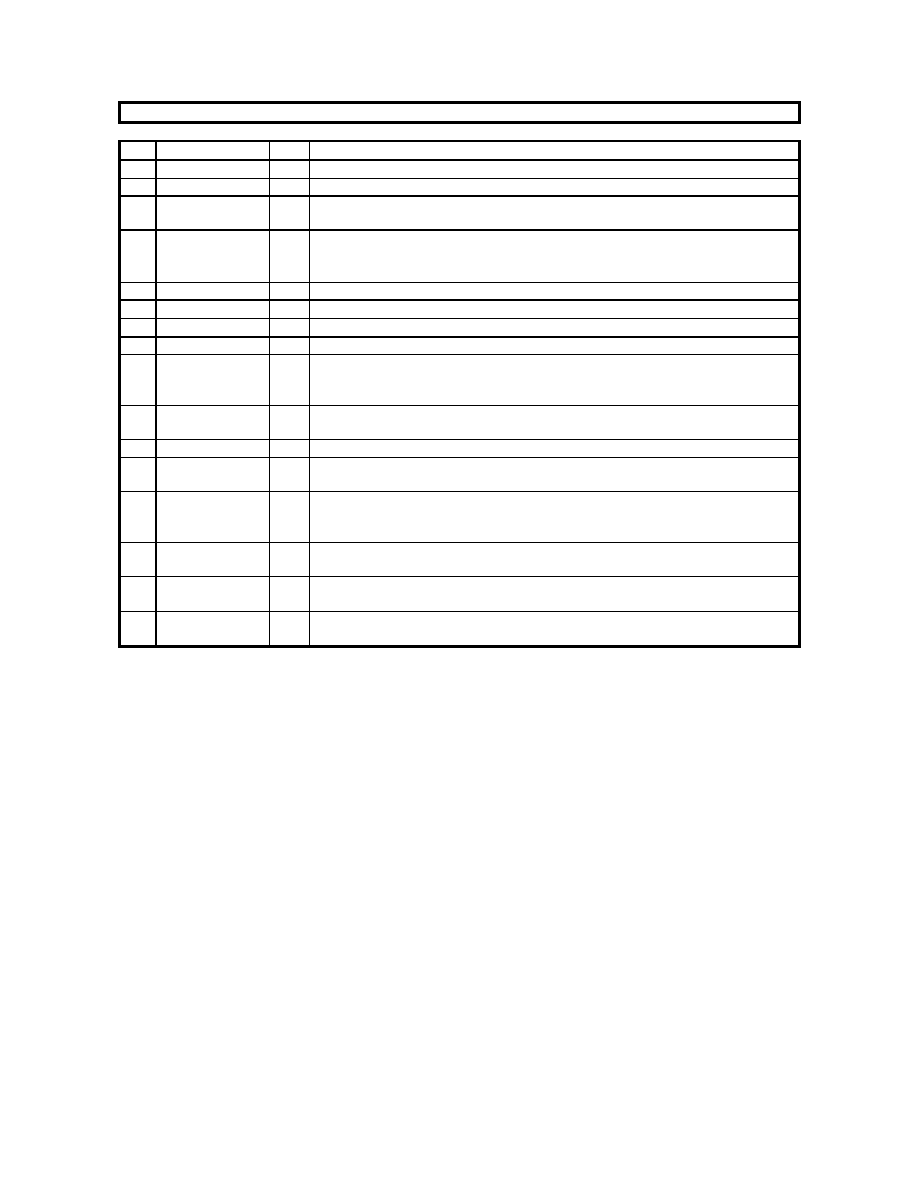
PIN/FUNCTION
No.
Pin Name
I/O
Description
1
AINR
I
Rch Analog Input Pin
2
AINL
I
Lch Analog Input Pin
3
NC
-
NC Pin
No internal bonding.
4
VCOM
O
Common Voltage Output Pin
Normally connected to AGND with a 0.1
µ
F ceramic capacitor in parallel with an
electrolytic capacitor less than 2.2
µ
F.
5
AGND
-
Analog Ground Pin, 0V
6
VA
-
Analog Power Supply Pin, +4.5
+5.5V
7
VD
-
Digital Power Supply Pin, +2.7
+5.5V(fs=48kHz), +4.5
+5.5V(fs=96kHz)
8
DGND
-
Digital Ground Pin, 0V
9
SDTO
O
Serial Data Output Pin
Data bits are presented MSB first, in 2's complement format.
This pin is "L" in the power-down mode.
10
LRCK
I
Left/Right Channel Select Pin
The fs clock is input to this pin.
11
MCLK
I
Master Clock Input Pin
12
SCLK
I
Serial Data Input Pin
Output data is clocked out on the falling edge of SCLK.
13
PDN
I
Power-Down Pin
When "L", the circuit is in power-down mode.
The AK5380 should always be reset upon power-up.
14
DIF
I
Serial Interface Format Pin
"L": MSB justified, "H": I
2
S
15
TTL
I
Digital Input Level Select Pin
"L": CMOS level (VD=2.7
5.5V), "H": TTL level (VD=4.5
5.5V)
16
TST
I
Test Pin (Internal pull-down pin)
This pin should be left open.
Note: All input pins except pull-down pins should not be left floating.
ASAHI KASEI
[AK5380]
MS0100-E-00
2001/5
- 4 -
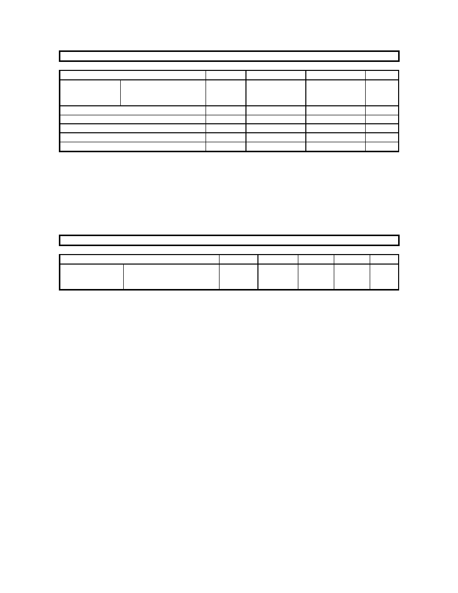
ABSOLUTE MAXIMUM RATINGS
(AGND, DGND=0V; Note 1)
Parameter
Symbol
min
max
Units
Power Supplies
Analog (VA pin)
Digital (VD pin)
|AGND-DGND|
VA
VD
GND
-0.3
-0.3
-
6.0
6.0
0.3
V
V
V
Input Current (any pins except for supplies)
IIN
-
±
10
mA
Analog Input Voltage (AINL, AINR pins)
VINA
-0.3
VA+0.3
V
Digital Input Voltage
VIND
-0.3
VD+0.3
V
Ambient Temperature
Ta
-40
85
∞
C
Storage Temperature
Tstg
-65
150
∞
C
Notes:
1. All voltages with respect to ground.
2. AGND and DGND must be connected to the same analog ground plane.
WARNING: Operation at or beyond these limits may results in permanent damage to the device.
Normal operation is not guaranteed at these extremes.
RECOMMENDED OPERATING CONDITIONS
(AGND, DGND=0V; Note 1)
Parameter
Symbol
min
typ
max
Units
Power Supplies
(Note 3)
Analog
Digital (fs=4kHz to 48kHz)
Digital (fs=4kHz to 96kHz)
VA
VD
VD
4.5
2.7
4.5
5.0
5.0
5.0
5.5
VA
VA
V
V
V
Notes:
1. All voltages with respect to ground.
3. The power up sequence between VA and VD is not critical.
*AKM assumes no responsibility for the usage beyond the conditions in this datasheet.

ASAHI KASEI
[AK5380]
MS0100-E-00
2001/5
- 5 -
ANALOG CHARACTERISTICS
(Ta=25
∞
C; VA,VD=5V; fs=48kHz; I/F format=Mode 0; Signal Frequency =1kHz;
Measurement band width=20Hz
20kHz; BW=40Hz
40kHz at fs=96kHz; unless otherwise specified)
Parameter
min
typ
max
Units
ADC Analog Input Characteristics:
Resolution
24
Bits
S/(N+D) (-1dBFS) (Note 4)
fs=48kHz
fs=96kHz
88
82
96
90
dB
dB
DR (-60dBFS) (Note 5)
fs=48kHz, A-weighted
fs=96kHz
100
94
106
102
dB
dB
S/N
fs=48kHz, A-weighted
fs=96kHz
100
94
106
102
dB
dB
Interchannel Isolation
90
110
dB
DC Accuracy
Interchannel Gain Mismatch
0.1
0.5
dB
Gain Drift
100
150
ppm/
∞
C
Input Voltage (Note 6)
fs=48kHz
2.8
3.0
3.2
Vpp
fs=96kHz
3.0
3.2
3.4
Vpp
Input Resistance (Note 7)
10
15
k
Power Supply Rejection (Note 8)
-
50
dB
Power Supplies
Power Supply Current (VA+VD)
Normal Operation (PDN= "H", fs=48kHz) (Note 9)
Normal Operation (PDN= "H", fs=96kHz) (Note 9)
Power-Down Mode (PDN= "L")
24
30
10
36
45
100
mA
mA
µ
A
Notes:
4. The ratio of the rms value of the signal to the rms sum of all the spectral components less than 20kHz bandwidth,
including distortion components.
5. S/(N+D) which is measured with an input signal of -60dB below full-scale.
6. This value is the full scale(0dB) of the input voltage. Input voltage is proportional to VA. (Vin=0.6xVA)
7. 9k
(typ) and 6k
(min) at fs=96kHz.
8. PSR is applied to VA,VD with 1kHz, 50mVpp.
9. VA=16mA(typ); VD=8mA(typ)@48kHz&5V, 5mA(typ)@48kHz&3V, 14mA(typ)@96kHz&5V.