 | –≠–ª–µ–∫—Ç—Ä–æ–Ω–Ω—ã–π –∫–æ–º–ø–æ–Ω–µ–Ω—Ç: AK5366VQ | –°–∫–∞—á–∞—Ç—å:  PDF PDF  ZIP ZIP |
ASAHI KASEI
[AK5366]
MS0309-E-00
2004/05
- 1 -
GENERAL DESCRIPTION
AK5366 is a high-performance 24-bit, 48kHz sampling ADC for consumer audio and digital recording
applications. Thanks to AKM's Enhanced Dual-Bit modulator architecture, this analog-to-digital converter
has an impressive dynamic range of 103dB with a high level of integration. The AK5366 has a 5-channel
stereo input selector, an input Programmable Gain Amplifier with an ALC function. All this integration with
high-performance makes the AK5366 well suited for CD and DVD recording systems.
FEATURES
1. 24bit Stereo ADC
∑
5ch Stereo Inputs Selector
∑
Input PGA from +18dB to 0dB, 0.5dB Step
∑
Peak Hold Function
∑
Auto Level Control (ALC) Circuit
∑
Digital HPF for offset cancellation (fc=1.0Hz@fs=48kHz)
∑
Digital Attenuator from +8dB to
-
63dB, Mute
∑
Soft Mute
∑
Single-end Inputs
∑
S/(N+D) : 94dB
∑
DR, S/N : 103dB
∑
Audio I/F Format : 24bit MSB justified, I
2
S
2. 3-wire Serial
µ
P Interface / I
2
C-Bus
3. Master / Slave Mode
4. Master Clock : 256fs/384fs/512fs
5. Sampling Rate : 32kHz to 48kHz
6. Power Supply
∑
AVDD: 4.75
5.25V (typ. 5.0V)
∑
DVDD: 3.0
5.25V (typ. 3.3V)
∑
TVDD: 3.0
5.25V for input tolerant (typ. 5.0V)
7. Ta =
-
40
85
∞
C
8. Package : 44pin LQFP
9. AK5365 Semi-Pin Compatible
24-Bit 48kHz
ADC with Selector/PGA/ALC
AK5366
ASAHI KASEI
[AK5366]
MS0309-E-00
2004/05
- 2 -
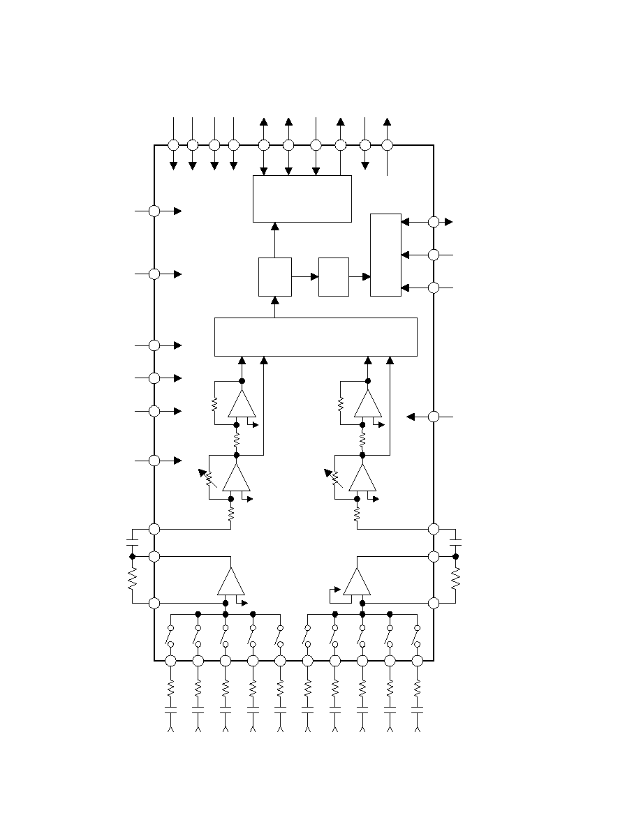
Block Diagram
LIN1
LIN2
LIN3
LIN4
LIN5
RIN1
RIN2
RIN3
RIN4
RIN5
ADC
IPGAL
ROPIN
ROUT
IPGAR
Control Register
I/F
CSN
CAD1
CCLK
SCL
CDTI
SDA
LOPIN
M/S
PDN
LOUT
IPGA
IPGA
I2C
(ALC)
(ALC)
SMUTE
Pre-Amp
Pre-Amp
HPF
DATT
Peak
Hold
VCOM
TVDD
LRCK
BICK
MCLK
SDTO
AVSS
AVDD
DVSS
DVDD
Audio I/F
Controller
SEL2 SEL1 SEL0
Block diagram

ASAHI KASEI
[AK5366]
MS0309-E-00
2004/05
- 3 -
Ordering Guide
AK5366VQ
-40 +85∞C
44pin
LQFP
(0.8mm
pitch)
AKD5366
Evaluation
Board
for
AK5366
Pin Layout
LIN5
RI
N5
44 43
1
42 41 40 39 38 37 36 35 34
33
32
31
30
29
28
27
26
25
24
23
22
21
20
19
18
17
16
15
14
13
12
2
3
4
5
6
7
8
9
10
11
AK5366VQ
Top View
TEST1
LIN4
TEST2
LIN3
TEST3
LIN2
TEST4
LIN1
LOPIN
LOUT
IP
GA
L
IP
GA
R
RO
UT
RO
PI
N
AVDD
AVSS
VCO
M
DVSS
DVDD
SDT
O
BI
CK
LRCK
MCLK
PDN
TVDD
SMUTE
SEL0
SEL1
SEL2
CDTI/SDA
CCLK/SCL
CSN/CAD1
T
EST
8
RI
N4
T
EST
7
RI
N3
T
EST
6
RI
N2
T
EST
5
RI
N1
M/
S
I2C

ASAHI KASEI
[AK5366]
MS0309-E-00
2004/05
- 4 -
Compatibility with AK5365
AK5365
AK5366
Pin 26
ALC
TVDD
Pin 34
CTRL
I2C
fs
max. 96kHz
max. 48kHz
ALC bit default value
"0" : ALC=OFF
"1" : ALC=ON
REF7-0 bit default value
"89H" : +4.5dB
"8EH" : +7.0dB
IPGA Gain
0dB
+12dB
0dB
+18dB
DATT Volume
-72dB 0dB
-63dB +8dB
MCLK AC Coupling Input
No
Yes
Peak Hold Circuit
No
Yes
I2C Speed
100kHz
400kHz
5V tolerant
No
Yes
(1) Pin Compatibility
AK5365
AK5366
Pin 26
ALC
TVDD
Pin 34
CTRL
I2C
(2) Software Compatibility
Addr Register
Name
D7
D6
D5
D4
D3
D2
D1
D0
00H Power Down & Reset Control
0
0
0
0
0
MCKPD
MCKAC
PWN
01H Input Selector Control
0
0
0
0
0
SEL2
SEL1
SEL0
02H
Clock & Format Control
0
0
0
0
DIF
CKS1
CKS0
SMUTE
03H Timer
Select
0
0
LTM1 LTM0
ZTM1
ZTM0 WTM1 WTM0
04H Lch IPGA Control
IPGL7
IPGL6
IPGL5
IPGL4
IPGL3
IPGL2
IPGL1
IPGL0
05H Rch
IPGA
Control
IPGR7
IPGR6
IPGR5 IPGR4
IPGR3
IPGR2 IPGR1 IPGR0
06H ALC Mode Control 1
0
0
ZELMN
ALC
FR
LMTH
RATT
LMAT
07H ALC Mode Control 2
REF7
REF6
REF5 REF4 REF3 REF2 REF1 REF0
08H Lch DATT Control
ATTL7
ATTL6
ATTL5
ATTL7
ATTL7
ATTL7
ATTL7
ATTL0
09H Rch DATT Control
ATTR7
ATTR6
ATTR5
ATTR4
ATTR3
ATTR2
ATTR1
ATTR0
0AH Lch Peak Hold Low Byte
PHL7
PHL6
PHL5
PHL4
PHL3
PHL2
PHL1
PHL0
0BH Lch Peak Hold High Byte
PHL15
PHL14
PHL13
PHL12
PHL11
PHL10
PHL9
PHL8
0CH Rch Peak Hold Low Byte
PHR7
PHR6
PHR5
PHR4
PHR3
PHR2
PHR1
PHR0
0DH Rch Peak Hold High Byte
PHR15
PHR14
PHR13
PHR12
PHR11
PHR10
PHR9
PHR8
: Changing points from AK5365's register.

ASAHI KASEI
[AK5366]
MS0309-E-00
2004/05
- 5 -
PIN/FUNCTION
No. Pin
Name
I/O
Function
1
LIN5
I
Lch Analog Input 5 Pin
2 TEST1
I
Test 1 Pin
This pin should be connected to AVSS.
3
LIN4
I
Lch Analog Input 4 Pin
4 TEST2
I
Test 2 Pin
This pin should be connected to AVSS.
5
LIN3
I
Lch Analog Input 3 Pin
6 TEST3
I
Test 3 Pin
This pin should be connected to AVSS.
7
LIN2
I
Lch Analog Input 2 Pin
8 TEST4
I
Test 4 Pin
This pin should be connected to AVSS.
9
LIN1
I
Lch Analog Input 1 Pin
10 LOPIN
I
Lch Feedback Resistor Input Pin
11 LOUT
O
Lch Feedback Resistor Output Pin
12 IPGAL
I
Lch IPGA Input Pin
13 IPGAR
I
Rch IPGA Input Pin
14 ROUT
O
Rch Feedback Resistor Output Pin
15 ROPIN
I
Rch Feedback Resistor Input Pin
16 AVDD
- Analog Power Supply Pin, 4.75
5.25V
17 AVSS
-
Analog Ground Pin
18 VCOM
O
Common Voltage Output Pin, AVDD/2
Bias voltage of ADC input.
19 DVSS
-
Digital Ground Pin
20 DVDD
- Digital Power Supply Pin, 3.0
5.25V
21 SDTO
O
Audio Serial Data Output Pin
22 BICK
I/O Audio Serial Data Clock Pin
Note: All digital input pins except pull-down pins should not be left floating.
Note: TEST1, TEST2, TEST3 and TEST4 pins should be connected to AVSS.