 | –≠–ª–µ–∫—Ç—Ä–æ–Ω–Ω—ã–π –∫–æ–º–ø–æ–Ω–µ–Ω—Ç: AK4632 | –°–∫–∞—á–∞—Ç—å:  PDF PDF  ZIP ZIP |
ASAHI KASEI
[AK4632]
MS0396-E-00
2005/06
-
1
-
GENERAL DESCRIPTION
The AK4632 is a 16-bit mono CODEC with Microphone-Amplifier, Speaker-Amplifier and Video-
Amplifier. Input circuits include a Microphone-Amplifier and an ALC (Automatic Level Control) circuit.
Output circuits include a Speaker-Amplifier and Mono Line Output. Video circuits include a LPF and
Video-Amplifier. The AK4632 suits a moving picture of Digital Still Camera and etc. This
speaker-Amplifier supports a Piezo Speaker. The AK4632 is housed in a space-saving 32-pin QFN
package.
FEATURE
1. 16-Bit Delta-Sigma Mono CODEC
2. Recording Function
∑
1ch Mono Input
∑
1
st
MIC Amplifier: 0dB, 20dB, 26dB or 32dB
∑
2
nd
Amplifier with ALC: -8dB
+27.5dB, 0.5dB Step
∑
ADC Performance: S/(N+D): 80dB, DR, S/N: 85dB
3. Playback Function
∑
Digital Volume: +12dB
-115dB, 0.5dB Step, Mute
∑
Mono Line Output Performance: S/(N+D): 85dB, S/N: 93dB
∑
Mono Speaker-Amp
-
Speaker-Amp
Performance:
S/(N+D):
60dB,
S/N:
90dB
(150mW@
8
)
- BTL Output
-
ALC
(Automatic
Level
Control)
Circuit
- Output Power: 400mW @ 8
, SVDD=3.3V
3.0Vrms@SVDD=5V
∑
Beep Input
4. Power Management
5. Video Function
∑
A Composite Video Input
∑
Gain Control (-1.0dB
+10.5dB, 0.5dB Step)
∑
Low Pass Filter
∑
A Video-Amp for Composite Video Signal(+6dB)
∑
DC Direct Output or Sag Compensation Output
6. Flexible PLL Mode:
∑
Frequencies:
11.2896MHz, 12MHz, 12.288MHz, 13.5MHz, 24MHz, 27MHz (MCKI pin)
1fs (FCK pin)
16fs, 32fs or 64fs (BICK pin)
7. EXT Mode:
∑
Frequencies: 256fs, 512fs or 1024fs (MCKI pin)
8. Sampling Rate:
∑
PLL Slave Mode (FCK pin) : 7.35kHz
~
26kHz
∑
PLL Slave Mode (BICK pin) : 7.35kHz
~
48kHz
∑
PLL Slave Mode (MCKI pin):
8kHz, 11.025kHz, 12kHz, 16kHz, 22.05kHz, 24kHz, 32kHz, 44.1kHz, 48kHz
∑
PLL Master Mode:
8kHz, 11.025kHz, 12kHz, 16kHz, 22.05kHz, 24kHz, 32kHz, 44.1kHz, 48kHz
AK4632
16-Bit
Mono CODEC with ALC & MIC/SPK/Video-AMP
ASAHI KASEI
[AK4632]
MS0396-E-00
2005/06
-
2
-
∑
EXT Slave Mode:
7.35kHz
~
48kHz (256fs), 7.35kHz
~
26kHz (512fs), 7.35kHz
~
13kHz (1024fs)
9. Output Master Clock Frequency: 256fs
10. Serial
µ
P Interface: 3-wire
11. Master / Slave Mode
12. Audio Interface Format: MSB First, 2's compliment
∑
ADC: DSP Mode, 16bit MSB justified, I
2
S
∑
DAC: DSP Mode, 16bit MSB justified, 16bit LSB justified, I
2
S
13. Ta = -10
70
∞
C
14. Power Supply
∑
CODEC: 2.6
3.6V (typ. 3.3V)
∑
Speaker-Amp: 2.6
5.25V (typ. 3.3V/5.0V)
∑
Video-Amp: 2.8
5.25V (typ. 3.3V/5.0V)
15. Power Supply Current: 23.5 mA (All Power ON)
16. Package: 32pin QFN
17. Register Compatible with AK4631
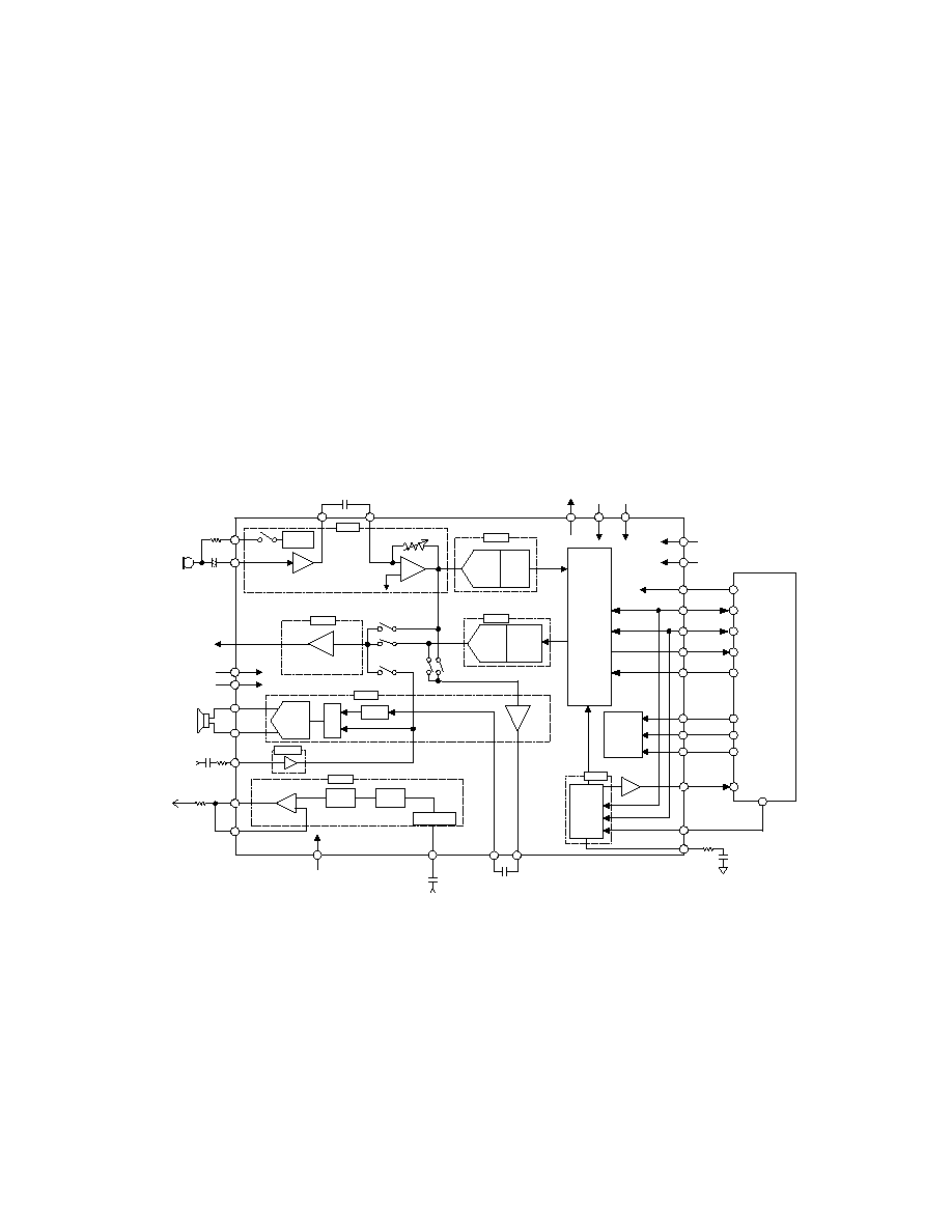
Block Diagram
PMMIC
AVDD
AVSS
MICOUT
AIN
Interface
Audio
MIC-AMP
0dB or 20dB
or 26dB or 32dB
MIC
MPI
MIC Power
Supply
HPF
ADC
ALC1
(IPGA)
PMADC
FCK
BICK
SDTO
SDTI
PDN
DSP
and
uP
CSN
CCLK
CDTI
SVDD
SVSS
PMDAC
DVOL
DAC
ALC2
MIN
MOUT
PMSPK
SPK-
AMP
SPP
SPN
ALC1M
MIX
AOUT
MCKI
MCKO
VCOC
PLL
PMPLL
PMAO
DACA
ALC1A
DACM
BEEPA
Control
Register
DVSS
DVDD
VCOM
BEEP
PMBP
VIN
VOUT
VSAG
GCA
VVDD
PMV
CLAMP
LPF
+6dB
-1dB ~ +10.5dB
Step 0.5dB
Figure 1. AK4632 Block Diagram

ASAHI KASEI
[AK4632]
MS0396-E-00
2005/06
-
3
-
Ordering Guide
AK4632VN
-10 +70∞C
32pin
QFN
(0.5mm
pitch)
AKD4632
Evaluation
board
for
AK4632
Pin Layout
MOUT
AOUT
BEEP
AIN
MICOUT
MIC
MPI
VCOM
MIN
SV
S
S
S
V
DD
SP
P
SP
N
MC
KO
MC
KI
DV
S
S
V
COC
A
V
DD
A
VS
S
V
V
DD
V
IN
V
OUT
V
SA
G
P
DN
DVDD
BICK
FCK
SDTO
SDTI
CDTI
CCLK
CSN
AK4632VN
Top View
25
26
27
28
29
30
31
32
24
23
22
1
16
15
14
13
12
11
10
9
21
20
19
2
3
4
5
6
7
8
18
17
Compare with AK4632
Function AK4631 AK4632
Video Function
No
Yes
Package
28pin QFN (5.2mm x 5.2mm)
32pin QFN (5.0mm x 5.0mm)
The audio function of the AK4632 is compatible with that of the AK4631. Since the register map of audio
function is the same as the AK4631's, the software of the audio function can run on the ak4632 without any
change.

ASAHI KASEI
[AK4632]
MS0396-E-00
2005/06
-
4
-
PIN/FUNCTION
No. Pin
Name
I/O
Function
1 VCOC
O
Output Pin for Loop Filter of PLL Circuit
This pin should be connected to AVSS with one resistor and capacitor in series.
2
AVDD
-
Analog Power Supply Pin
3
AVSS
-
Analog Ground Pin
4
VVDD
-
Video Block Power Supply Pin.
5
VIN
I
Composite Video Signal Input Pin
6
VOUT
O
Composite Video Signal Driver Pin
7
VSAG
I
Composite Video Signal Output Feedback Input Pin
8 PDN
I
Power-Down Mode Pin
"H": Power up, "L": Power down reset and initialize the control register.
9 CSN
I Chip
Select
Pin
10 CCLK
I
Control Data Clock Pin
11 CDTI
I
Control Data Input Pin
12 SDTI
I
Audio Serial Data Input Pin
13 SDTO
O
Audio Serial Data Output Pin
14 FCK
I/O Frame Clock Pin
15 BICK
I/O Audio Serial Data Clock Pin
16 DVDD
-
Digital Power Supply Pin
17 DVSS
-
Digital Ground Pin
18 MCKI
I
External Master Clock Input Pin (Internal Pull Down 25k
@PDN pin ="L")
19 MCKO
O
Master Clock Output Pin
20 SPN
O
Speaker Amp Negative Output Pin
21 SPP
O
Speaker Amp Positive Output Pin
22 SVDD
-
Speaker Amp Power Supply Pin
23 SVSS
-
Speaker Amp Ground Pin
24 MIN
I ALC2
Input
Pin
25 MOUT
O
Mono Analog Output Pin
26 AOUT
O
Mono Line Output Pin
27 BEEP
I
Beep Signal Input Pin
28 AIN
I
IPGA (ALC1) Input Pin
29 MICOUT
O
Microphone Analog Output Pin
30 MIC
I
Microphone Input Pin (Mono Input)
31 MPI
O
MIC Power Supply Pin for Microphone
32 VCOM
O
Common Voltage Output Pin. Common Voltage = 0.45 x AVDD
Bias voltage of ADC inputs and DAC outputs.
Note : All input pins except analog input pins (MIC, AIN, MIN, BEEP and VIN pins) should not be left floating.
Note : The exposed pad on the bottom surface of the package must be open.

ASAHI KASEI
[AK4632]
MS0396-E-00
2005/06
-
5
-
Handling of Unused Pin
The unused I/O pins should be processed appropriately as below.
Classification Pin
Name
Setting
Analog Input
MIC, AIN, BEEP, MIN, VSAG
These pins should be open and each path
should be switched off.
Analog Output MICOUT, MPI, AOUT, MOUT, SPP, SPN, VOUT
These pins should be open.
Digital Input
MCKI, SDTI, FCK(when M/S bit =
"0"),
BICK(when M/S bit =
"0")
These pins should be connected to DVSS.
Digital Output
MCKO, SDTO, FCK(when M/S bit =
"1"),
BICK(when M/S bit =
"1")
These pins should be open.
ABSOLUTE MAXIMUM RATINGS
(AVSS, DVSS, SVSS=0V; Note 1)
Parameter Symbol
min
max
Units
Power Supplies:
Analog
Digital
Speaker-Amp
Video
|AVSS ≠ DVSS| (Note 2)
|AVSS ≠ SVSS| (Note 2)
AVDD
DVDD
SVDD
VVDD
GND1
GND2
-0.3
-0.3
-0.3
-0.3
-
-
6.0
6.0
6.0
6.0
0.3
0.3
V
V
V
V
V
V
Input Current, Any Pin Except Supplies
IIN
-
±10 mA
Analog Input Voltage(Audio) (Note 3)
VINA
-0.3 AVDD+0.3 V
Analog Input Voltage(Video) (Note 4)
VINV
-0.3 VVDD+0.3 V
Digital Input Voltage
VIND
-0.3 DVDD+0.3 V
Ambient Temperature (powered applied)
Ta
-10 70
∞C
Storage Temperature
Tstg
-65 150
∞C
Maximum Power Dissipation (Note 5)
Pd
-
700
mW
Note 1. All voltages with respect to ground.
Note 2. AVSS, DVSS and SVSS must be connected to the same analog ground plane.
Note 3. MIC, AIN, BEEP, MIN pins
Note 4. VIN pin
Note 5. In case that PCB wiring density is 100%. This power is the AK4632 internal dissipation that does not include
power of externally connected speaker.
WARNING: Operation at or beyond these limits may result in permanent damage to the device.
Normal operation is not guaranteed at these extremes.