
ASAHI KASEI
[AK4584]
MS0118-J-01
2001/11
- 1 -
AK4584
24
96kHz
24bit CODEC
ADC
DAC
AK4584
24
192kHz
(DIT)
(DIR)
AC-3/MPEG
Non-PCM
ADC
AK4584
PGA
MD, DVD-R, CD-R
*AC-3Dolby Laboratories
1. 24bit 2ch ADC
�
fs: max 96kHz
�
Single-end Input
�
S/(N+D): 90dB
�
Dynamic Range, S/N: 100dB
�
Digital HPF for offset cancellation
�
Input PGA with +18dB gain & 0.5dB step
�
Input DATT with �72dB ATT
�
I/F format: MSB justified or I
2
S
2. 24bit 2ch DAC
�
fs: max 192kHz
�
24bit 8 times Digital Filter
- Ripple:
�
0.005dB, Attenuation: 75dB
�
Single-end Output
�
S/(N+D): 94dB
�
Dynamic Range, S/N: 104dB
�
De-emphasis for 32kHz, 44.1kHz, 48kHz sampling
�
Digital Attenuator with soft-transition
�
Soft Mute
�
Zero Detect Function
�
I/F format: MSB justified, LSB justified or I
2
S
3. 3 Outputs 24 bit 192kHz DIT
�
3-Channel Transmission Outputs (2 Through outputs & DIT Output)
�
40 Bits Channel Status Buffer
24Bit 96kHz Audio CODEC with DIT/DIR
AK4584

ASAHI KASEI
[AK4584]
MS0118-J-01
2001/11
- 2 -
4. 4 Inputs 24bit 192kHz DIR
�
Supports AES3, IEC60958, S/PDIF, EIAJ CP1201
�
Low Jitter Analog PLL
�
PLL Lock Range: 32k
192kHz
�
Clock Source: PLL or X'tal
�
4 Channels Receiver Inputs
�
Detect Function
- Non-PCM Bit Stream Detection
- DTS-CD Bit Stream Detection
- Validity Flag Detection
- Sampling Frequency Detection
- Unlock & Parity Error Detection
�
40 bits Channel Status Buffer
�
Burst Preamble bit Pc, Pd Buffer for Non-PCM bit Stream
5. Support External Audio Clock Input
�
Master Clock Input
- 256fs, 384fs, 512fs, 768fs (fs = 44.1kHz
48kHz)
- 256fs, 384fs (fs = 88.2kHz
96kHz)
- 128fs, 192fs (fs = 176.4kHz
192kHz)
6. Support Master & Slave Mode
7. Serial
�
P I/F: 4-wire serial
8. 5V operation
9. 3V Power Supply Pin for 3V I/F
10. 44pin LQFP Package
11. Ta: -10 to 70�C
ASAHI KASEI
[AK4584]
MS0118-J-01
2001/11
- 3 -
n
DIR
RX2
IPGA
DATT
ADC
R_LRCK
R_BICK
R_DATA
R_MCLK
A_LRCK
A_BICK
A_DATA
A_MCLK
HPF
D_LRCK
D_BICK
D_DATA
D_MCLK
DATT
SMUTE
DAC
DIT
T_LRCK
T_BICK
T_DATA
T_MCLK
RX3
RX4
LIN
RIN
ROUT
LOUT
TX3
TX1
LRCK
BICK
SDTO
SDTI
MCKO1
Audio
Interface
RX2
RX3
RX4
LIN
RIN
TX2
TX3
TX1
TX2
LOUT
ROUT
LRCK
BICK
SDTO
SDTI
AVDD
AVSS
DVDD
DVSS
TVDD
PVDD
PVSS
VREF
VCOM
DZF
M/S
INT0
PDN
Control Register
CDTO CDTI CCLK CSN
MCLK
Selector
Divider
MCKI
MCKO1
R
XTI
XTO
X'tal
OSC
TX1E
TX2E
TX3E
OPS1-0
IPS1-0
RX1
RX1
INT1
MCKO2
MCKO2 DMCK XTALE
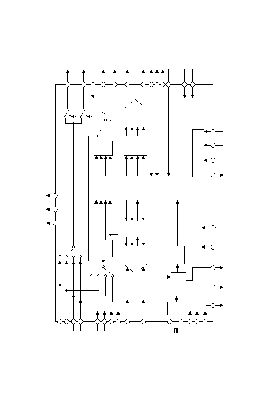
Block Diagram

ASAHI KASEI
[AK
4584]
MS0118-J-01
2001/11
- 4 -
n
AK4584VQ
-
10
+70
�
C
44pin LQFP (0.8mm pitch)
AKD4584
AK4584
n
TEST2
RX2
44 43
1
42 41 40 39 38 37 36 35 34
33
32
31
30
29
28
27
26
25
24
23
22
21
20
19
18
17
16
15
14
13
12
2
3
4
5
6
7
8
9
10
11
AK4584VQ
Top View
RX3
NC
RX4
PDN
INT0
INT1
CDTI
CDTO
CCLK
CSN
TEST3
TX1
TX2
XTALE
TX3
DVDD
DVSS
TVDD
XTO
XTI/MCKI
DMCK
MCKO1
MCKO2
SDTO
SDTI
BICK
LRCK
M/S
DZF
VCOM
LOUT
ROUT
TEST1
RX1
PVSS
R
PVDD
LIN
RIN
VREF
AVDD
AVSS

ASAHI KASEI
[AK
4584]
MS0118-J-01
2001/11
- 5 -
No. Pin Name
I/O
Function
1
TEST2
I
Test 2 Pin (Internal pull-down pin)
2
RX3
I
Receiver Input 3 with Amp for 0.2Vpp
3
NC
I
NC Pin (No Internal bonding pin, Fixed to "AVSS")
4
RX4
I
Receiver Input 4 with Amp for 0.2Vpp
5
PDN
I
Power-Down Mode Pin
"H": Power up, "L": Power down reset and initialize the control register.
6
INT0
O
Interrupt 0 Pin
7
INT1
O
Interrupt 1 Pin
8
CDTI
I
Control Data Input Pin
9
CDTO
O
Control Data Output Pin
10
CCLK
I
Control Data Clock Pin
11
CSN
I
Chip Select Pin
12
TEST3
I
Test 3 Pin (Fixed to AVSS)
13
TX1
O
Transmitter 1 Output Pin
14
TX2
O
Transmitter 2 Output Pin
15
XTALE
I
X'tal Osc Enable Pin
"H" : Enable, "L" : Disable
16
TX3
O
Transmitter 3 Output Pin
17
DVDD
-
Digital Power Supply Pin, 4.75
5.25V
18
DVSS
-
Digital Ground Pin
19
TVDD
-
Output Buffer Power Supply Pin, 2.7
5.25V
20
XTO
O
X'tal Output Pin
XTI
I
X'tal Input Pin
21
MCKI
I
External Master Clock Input Pin
22
DMCK
I
MCKO1 Disable Pin
"H" : MCKO1 "L" output, "L" : MCKO1 output