 | –≠–ª–µ–∫—Ç—Ä–æ–Ω–Ω—ã–π –∫–æ–º–ø–æ–Ω–µ–Ω—Ç: AK4565VF | –°–∫–∞—á–∞—Ç—å:  PDF PDF  ZIP ZIP |
ASAHI KASEI
[AK4565]
MS0132-E-01
2003/05
- 1 -
GENERAL DESCRIPTION
The AK4565 is a low power voltage, 20bit CODEC. The recording feature includes four stereo inputs
selector which switches among microphone and line inputs etc. And the input PGA has an ALC function,
making it suitable for microphone application. The AK4565 has a dedicated power supply pin for digital
I/F, which can support I/O level down to 1.5V. The AK4565 can be powered-down partly and is suitable
for portable application.
FEATURES
1. Resolution: 20bits
2. Recording Functions
∑
Four Stereo Inputs Selector
∑
Input PGA (Programmable Gain Amplifier) with ALC (Automatic Level Control)
∑
FADEIN / FADEOUT
∑
Digital HPF for DC-offset cancellation (fc=3.7Hz@fs=48kHz)
3. Playback Function
∑
Digital De-emphasis Filter (tc = 50/15
µ
s, fs=32k, 44.1k and 48kHz)
4. Power Management
5. CODEC
∑
Single-ended Inputs/Outputs
∑
Input / Output Level: 1.5Vpp@VREF=2.5V (= 0.6 x VREF)
∑
S/(N+D): 83dB(ADC), 86dB(DAC) @VREF=2.5V
∑
DR, S/N: 87dB(ADC), 91dB(DAC) @VREF=2.5V
6. Master Clock: 256fs/384fs
7. Sampling Rate: 8kHz
50kHz
8. Audio Data Interface Format: MSB-First, 2's compliment
∑
ADC: 20bit MSB justified, I
2
S
∑
DAC: 20bit MSB justified, 16/20bit LSB justified, I
2
S
9.
µ
P Interface: 4-wire
10. Power Supply
∑
CODEC, IPGA: 2.3
3.6V (typ.2.5V)
∑
Digital I/F: 1.5
3.6V(typ.2.5V)
11. Power Supply Current
∑
ALL Power ON: 12.5mA
∑
IPGA + ADC: 8mA
∑
DAC: 5.5mA
12. Ta = - 40
85 ∫ C
13. Package: 28pin VSOP
14. AK4563A pin-compatible
Low Power 20bit CODEC with built-in ALC
AK4565

ASAHI KASEI
[AK4565]
MS0132-E-01
2003/05
- 2 -
INTL0
VCOM
LOUT
VA
AGND
CSN CCLK CDTI
MCLK
SDTO0
BCLK
LRCK
DGND
VT
VD
ADC
DAC
HPF
De-emp
Audio I/F
Controller
Control Register I/F
Clock Divider
PDN
SDTI
CDTO
INTL1
EXTL
INTR0
INTR1
EXTR
ROUT
IPGA
LIN
RIN
VREF
SDTO1
Figure 1. AK4565 Block Diagram
ASAHI KASEI
[AK4565]
MS0132-E-01
2003/05
- 3 -
n
Ordering Guide
AK4565VF -40
+85
∞
C 28pin VSOP (0.65mm pitch)
AKD4565 Evaluation board for AK4565
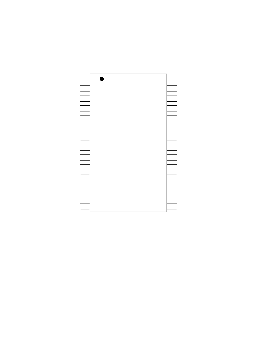
n
Pin Layout
EXTL
LOUT
ROUT
INTL1
INTR1
INTL0
INTR0
EXTR
LIN
RIN
VCOM
AGND
VA
VREF
VD
DGND
VT
SDTO0
LRCK
MCLK
BCLK
CDTO
CDTI
CSN
CCLK
PDN
SDTO1
SDTI
1
2
3
4
5
6
7
8
9
10
11
12
13
14
15
16
17
18
19
20
21
22
23
24
25
26
27
28
AK4565
Top
View
ASAHI KASEI
[AK4565]
MS0132-E-01
2003/05
- 4 -
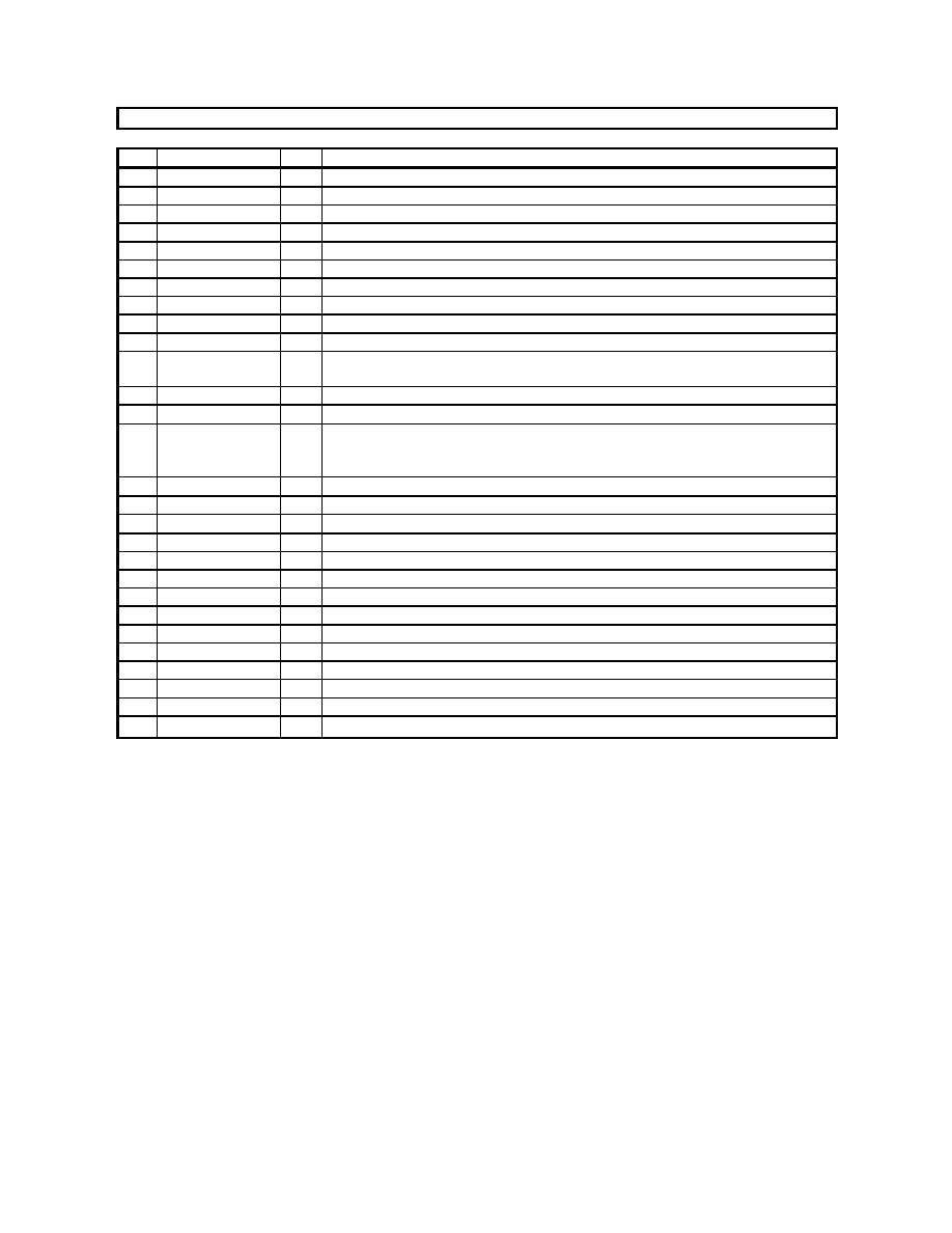
PIN / FUNCTION
No. Pin Name
I/O
Function
1
LOUT
O
Lch Analog Output Pin
2
ROUT
O
Rch Analog Output Pin
3
INTL1
I
Lch INT #1 Input Pin
4
INTR1
I
Rch INT #1 Input Pin
5
INTL0
I
Lch INT #0 Input Pin
6
INTR0
I
Rch INT #0 Input Pin
7
EXTL
I
Lch EXT Input Pin
8
EXTR
I
Rch EXT Input Pin
9
LIN
I
Lch Line Input Pin
10 RIN
I
Rch Line Input Pin
11 VCOM
O
Common Voltage Output Pin, 0.45 x VA
Bias voltage of ADC inputs and DAC outputs
12 AGND
-
Analog Ground Pin
13 VA
-
Analog Power Supply Pin, +2.3
3.6V
14 VREF
I
ADC & DAC Voltage Reference Input Pin, VA
Used as a voltage reference of ADC & DAC. VREF is connected externally to fltered
VA.
15 VD
-
Digital Power Supply Pin, +2.3
3.6V
16 DGND
-
Digital Ground Pin
17 VT
-
Digital I/F Power Supply Pin, +1.5
3.6V
18 SDTO0
O
Audio Serial Data #0 Output Pin
19 SDTO1
O
Audio Serial Data #1 Output Pin
20 SDTI
I
Audio Serial Data Input Pin
21 LRCK
I
Input/Output Channel Clock Pin
22 MCLK
I
Master Clock Input Pin
23 BCLK
I
Audio Serial Data Clock Pin
24 CDTO
O
Control Data Output Pin
25 CDTI
I
Control Data Input Pin
26 CSN
I
Chip Select Pin
27 CCLK
I
Control Data Clock Pin
28 PDN
I
Power Down & Reset Pin, "L": Power Down & Reset, "H": Normal Operation
Note: All digital input pins should not be left floating.

ASAHI KASEI
[AK4565]
MS0132-E-01
2003/05
- 5 -
ABSOLUATE MAXIMUM RATING
(AGND, DGND=0V; Note 1)
Parameter
Symbol
min
max
Units
Power Supply
Analog (VA pin)
Digital 1 (VD pin)
Digital 2 (VT pin)
| DGND ≠ AGND | (Note 2)
VA
VD
VT
GND
-0.3
-0.3
-0.3
-
4.6
4.6
4.6
0.3
V
V
V
V
Input Current, Any Pin Except Supplies
IIN
-
±
10
mA
Analog Input Voltage (Note 3)
VINA
-0.3
VA+0.3
V
Digital Input Voltage (Note 4)
VIND
-0.3
VT+0.3
V
Ambient Temperature
Ta
-40
85
∞
C
Storage Temperature
Tstg
-65
150
∞
C
Note 1. All voltages with respect to ground.
Note 2. AGND and DGND must be connected to the same analog plane.
Note 3. INTL0, INTR0, INTL1, INTR1, EXTL, EXTR, LIN, RIN and VREF pins
Note 4. PDN, MCLK, BCLK, LRCK, SDTI, CSN, CCLK and CDTI pins
WARNING: Operation at or beyond these limits may result in permanent damage to the device.
Normal operation is not guaranteed at these extremes.
RECOMMENDED OPERATING CONDITIONS
(AGND, DGND=0V; Note 1)
Parameter
Symbol
min
typ
max
Units
Power Supply
Analog (VA pin)
Digital 1 (VD pin) (Note 5)
Digital 2 (VT pin)
VA
VD
VT
2.3
2.3 or VA-0.3
1.5
2.5
2.5
2.5
3.6
VA
VD
V
V
V
Reference Voltage
Analog Reference Voltage
(VREF pin) (Note 6)
VREF
-
-
VA
V
Note 1. All voltages with respect to ground.
Note 5. Minimum value is the higher between 2.3V and "VA-0.3"V.
Note 6. VREF and VA should be the same voltage.
WARNING: AKM assumes no responsibility for the usage beyond the conditions in this datasheet.