 | –≠–ª–µ–∫—Ç—Ä–æ–Ω–Ω—ã–π –∫–æ–º–ø–æ–Ω–µ–Ω—Ç: AK4525VF | –°–∫–∞—á–∞—Ç—å:  PDF PDF  ZIP ZIP |
ASAHI KASEI
[AK4525]
MS0053-E-00
2000/9
- 1 -
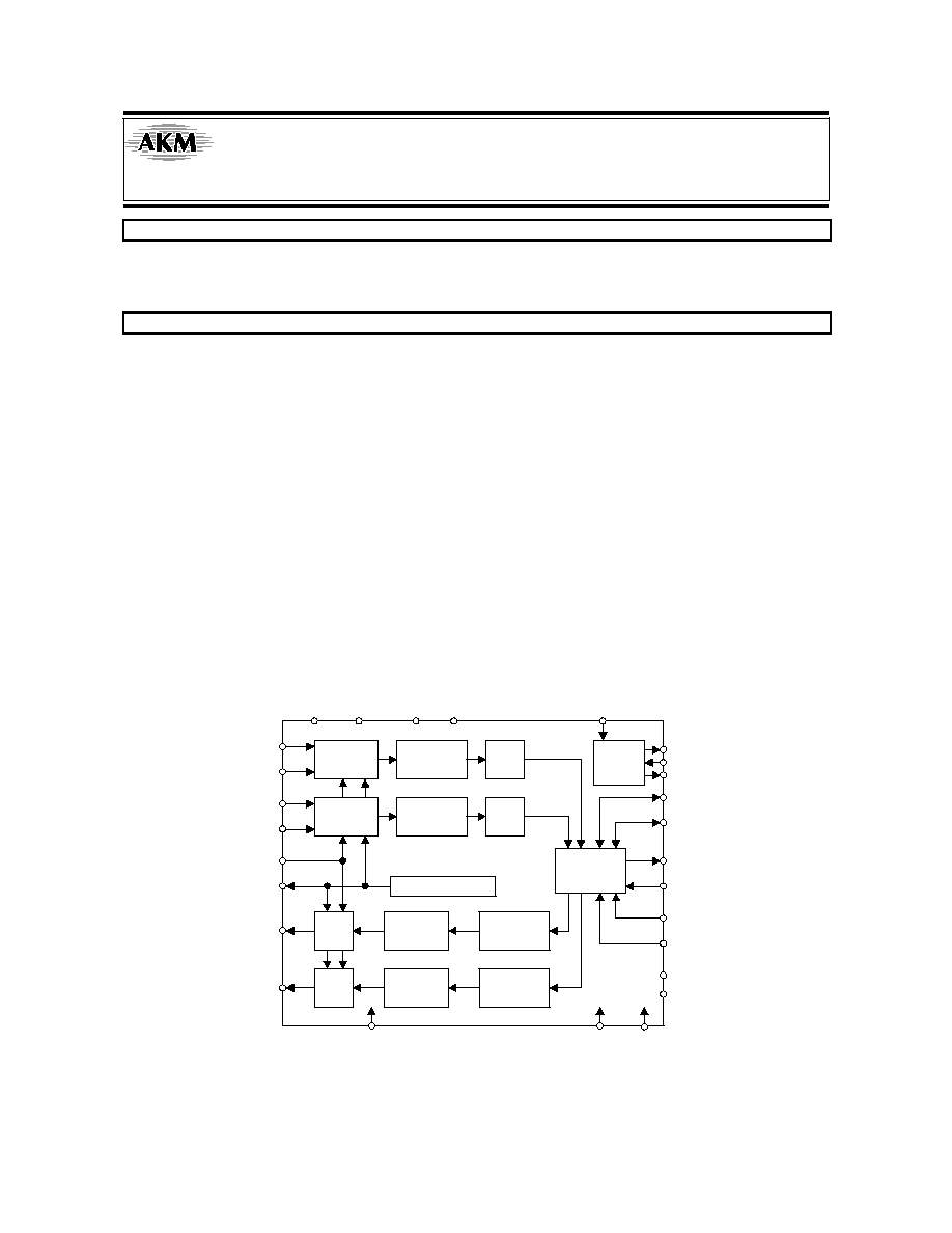
GENERAL DESCRIPTION
The AK4525 has a dynamic range of 100dB and is well-suited middle-range MD, surround system,
musical instruments and car audio. Analog inputs are full-differential with single-end capability. Analog
outputs are single-ended. The AK4525 has X' tal oscillation circuit and master mode.
FEATURES
o
Stereo ADC
- 64x Oversampling
- Sample Rate Ranging from 32kHz to 48kHz
- S/(N+D): 92dB
- Dynamic range, S/N: 100dB
- Digital HPF for offset cancellation
o
Stereo DAC
- 128x Oversampling
- Sampling Rate Ranging from 32kHz to 48kHz
- 2nd order SCF + 2nd order CTF
- Digital de-emphasis for 32kHz, 44.1kHz, 48kHz sampling
- S/(N+D): 90dB
- Dynamic Range, S/N: 100dB
- Soft Mute
o
High Jitter Tolerance
o
Master Clock: 256fs, 384fs, 512fs
o
X' tal Oscillation circuit
o
Master/Slave Mode
o
Analog Power Supply: 4.5 to 5.5V, Digital Power Supply: 3.1 to 5.5V
VA
AGND
VD DGND
CMODE
AINL+
AINL-
AINR+
AINR-
VREFH
VCOM
AOUTL
AOUTR
MCKO
LRCK
SCLK
SDTO
SDTI
DIF0
DIF1
SMUTE
DEM1
DEM0
PDN
Modulator
Modulator
Filter
Decimation
Filter
Decimation
HPF
HPF
Common Voltage
LPF
LPF
Modulator
Modulator
Interpolator
8x
Interpolator
8x
Serial I/O
Interface
Clock
Divider
M/S
Gen &
XTI
XTO
20Bit Stereo
ADC & DAC with X
'
tal Osc
AK4525

ASAHI KASEI
[AK4525]
MS0053-E-00
2000/9
- 2 -
n
Ordering Guide
AK4525VF
-40
+85
∞
C
28pin VSOP (0.65mm pitch)
AKD4525
Evaluation Board for AK4525
n
Pin Layout
AGND
VREFH
AINR+
AINR-
AINL+
AINL-
VA
XTI
XTO
DIF0
DIF1
LRCK
SCLK
SDTI
SDTO
SMUTE
DEM0
DEM1
MCKO
VD
DGND
PDN
CMODE
AOUTL
AOUTR
VCOM
TST
M/S (Internal Pull-down)
1
2
3
4
5
6
7
8
9
10
11
12
13
14
15
16
17
18
19
20
21
22
23
24
25
26
27
28
AK4525
Top
View
n
Difference with AK4522 and AK4523
AK4522
AK4523
AK4525
Crystal Oscillator
Not available
Not available
Available
Master Mode
Not available
Not available
Available
Digital Power Supply
2.7
5.5V
3.0
5.5V
3.1
5.5V
Ambient Operating
-10
70
∞
C
-40
85
∞
C
-40
85
∞
C
Package
24pin VSOP
28pin VSOP
28pin VSOP
ASAHI KASEI
[AK4525]
MS0053-E-00
2000/9
- 3 -
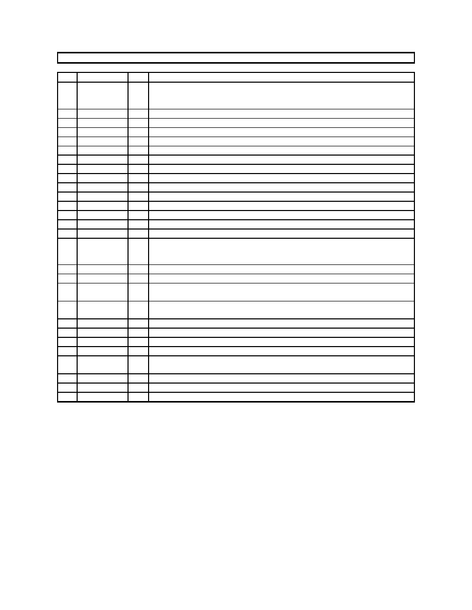
PIN/FUNCTION
No.
Pin Name
I/O
Function
1
VREFH
I
Positive Voltage Reference Input Pin, VA
Used as a positive voltage reference by ADC & DAC. VREFH should be connected
externally to filtered VA.
2
AINR+
I
Rch Analog Positive Input Pin
3
AINR-
I
Rch Analog Negative Input Pin
4
AINL+
I
Lch Analog Positive Input Pin
5
AINL-
I
Lch Analog Negative Input Pin
6
VA
-
Analog Power Supply Pin
7
AGND
-
Analog Ground Pin
8
XTI
I
X'tal Input Pin
9
XTO
O
X'tal Output Pin
10
DIF0
I
Audio Data Interface Format 0 Pin
11
DIF1
I
Audio Data Interface Format 1 Pin
12
LRCK
I/O
Input/Output Channel Clock Pin
13
SCLK
I/O
Audio Serial Data Clock Pin
14
SDTI
I
Audio Serial Data Input Pin
15
SDTO
O
Audio Serial Data Output Pin
16
SMUTE
I
Soft Mute Pin
When this pin goes "H", soft mute cycle is initiated.
When returning "L", the output mute releases.
17
DEM0
I
De-emphasis Frequency Select 0 Pin
18
DEM1
I
De-emphasis Frequency Select 1 Pin
19
TST
I
Test Pin
This pin must be connected to DGND.
20
M/S
I
Master/Slave Mode (Internal pull-down pin)
"H": Master mode, "L": Slave mode
21
MCKO
O
Master Clock Output Pin
22
VD
-
Digital Power Supply Pin
23
DGND
-
Digital Ground Pin
24
PDN
I
Power-Down Mode Pin
25
CMODE
I
Master Clock Select Pin (Internal biased pin)
"H": 384fs, "L": 256fs, "NC": 512fs
26
AOUTL
O
Lch Analog Output Pin
27
AOUTR
O
Rch Analog Output Pin
28
VCOM
O
Common Voltage Output Pin, VA/2
Note: All input pins except pull-down or biased pins should not be left floating.

ASAHI KASEI
[AK4525]
MS0053-E-00
2000/9
- 4 -
ABSOLUTE MAXIMUM RATINGS
(AGND, DGND=0V; Note 1)
Parameter
Symbol
min
max
Units
Power Supplies
Analog
Digital
|AGND-DGND| (Note 2)
VA
VD
GND
-0.3
-0.3
-
6.0
6.0
0.3
V
V
V
Input Current, Any Pin Except Supplies
IIN
-
±
10
mA
Analog Input Voltage
VINA
-0.3
VA+0.3
V
Digital Input Voltage
VIND
-0.3
VD+0.3
V
Ambient Temperature (power applied)
Ta
-40
85
∞
C
Storage Temperature
Tstg
-65
150
∞
C
Notes: 1. All voltages with respect to ground.
2. AGND and DGND must be same voltage.
WARNING: Operation at or beyond these limits may result in permanent damage to the device.
Normal operation is not guaranteed at these extremes.
RECOMMENDED OPERATING CONDITIONS
(AGND, DGND=0V; Note 1)
Parameter
Symbol
min
typ
max
Units
Power Supplies
(Note 3)
Analog
Digital
VA
VD
4.5
3.1
5.0
5.0
5.5
VA
V
V
Notes: 1. All voltages with respect to ground.
3. The power up sequence between VA and VD is not critical.
*AKM assumes no responsibility for the usage beyond the conditions in this datasheet.

ASAHI KASEI
[AK4525]
MS0053-E-00
2000/9
- 5 -
ANALOG CHARACTERISTICS
(Ta=25
∞
C; VA, VD=5.0V; AGND=DGND=0V; VREFH=VA; fs=44.1kHz; SCLK=64fs;
Signal Frequency =1kHz; 20bit Data; Measurement frequency = 10Hz
20kHz; unless otherwise specified)
Parameter
min
typ
max
Units
ADC Analog Input Characteristics: Differential Inputs; Analog Source Impedance=470
Resolution
20
Bits
S/(N+D) (-0.5dB Input) (Note 4)
84
92
dB
DR (-60dB Input, A-Weighted) (Note 5)
94
100
dB
S/N (A-Weighted) (Note 5, 6)
94
100
dB
Interchannel Isolation
90
110
dB
Interchannel Gain Mismatch
0.1
0.3
dB
Gain Drift
20
ppm/
∞
C
Input Voltage (AIN=0.6 x VREFH) (Note 7)
2.85
3.0
3.15
Vpp
Input Resistance
15
25
k
Power Supply Rejection (Note 8)
50
dB
DAC Analog Output Characteristics:
Resolution
20
Bits
S/(N+D)
80
90
dB
DR (-60dB Output, A-Weighted) (Note 5)
94
100
dB
S/N (A-Weighted) (Note 6, 9)
94
100
dB
Interchannel Isolation
90
110
dB
Interchannel Gain Mismatch
0.2
0.5
dB
Gain Drift
20
-
ppm/
∞
C
Output Voltage (AOUT=0.58 x VREFH)
2.65
2.9
3.15
Vpp
Load Resistance
5
k
Load Capacitance
25
pF
Power Supply Rejection (Note 8)
50
dB
Power Supplies VA=VD=5V
Analog, VA
PDN= "H"
40
55
mA
Digital, VD
PDN= "H"
12
20
mA
Power Down
PDN= "L" (Note 10)
6
12
mA
Notes: 4. In case of single ended input, S/(N+D)=80dB(typ, @VA=5V).
5. In case of 16bit, DR and S/N of ADC are 98dB. DR of DAC is 98dB.
6. S/N measured by CCIR-ARM is 96dB at each converter and 94dB at ADC to DAC loopback.
7. Full scale input for each AIN+/- pin is 1.5Vpp in differential mode.
8. PSR is applied to VA, VD with 1kHz, 50mVpp. VREFH pin is held a constant voltage.
9. As the input data is "0", S/N is 100dB regardless of resolution.
10. X'tal circuit is oscillating and all digital input pins are held VD or DGND.