ASAHI KASEI
[AK4116]
MS0156-E-02
2004/04
- 1 -
GENERAL DESCRIPTION
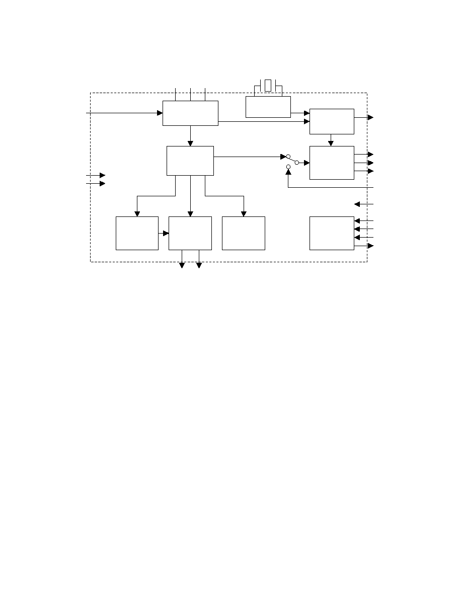
The AK4116 is a low power S/PDIF AES/EBU receiver supporting resolution up to 24-bit. The integrated
channel status decoder supports both consumer and professional modes. The AK4116 can automatically
detect a Non-PCM bit stream. Combining the AK4116 with a multi-channel codec such as AKM's
AK4527B or AK4529 can create a complete AC-3 system. Mode settings can be controlled via
microprocessor serial interface. The small 20pin QFN package saves board space.
*AC-3 is a trademark of Dolby Laboratories.
FEATURES
AES3, IEC60958, S/PDIF, EIAJ CP1201 Compatible
Low jitter Analog PLL
PLL Lock Range : 32kHz to 48kHz
Clock Source: PLL or X'tal
Auxiliary digital input
Detection Functions
- Non-PCM Bit Stream Detection
- DTS-CD Bit Stream Detection
- Sampling Frequency Detection (32kHz, 44.1kHz, 48kHz)
- Unlock & Parity Error Detection
- Validity Flag Detection
Up to 24bit Audio Data Format
Audio I/F: Left justified, Right justified (16bit, 18bit, 20bit, 24bit), I
2
S
40-bit Channel Status Buffer
Burst Preamble bit Pc and Pd Buffer for Non-PCM bit stream
Q-subcode Buffer for CD bit stream
4-wire Serial µP I/F
Master Clock Output: 256fs
Operating Voltage: 2.7 to 3.6V
Power Supply Current: 7mA (PLL mode)
2mA (X'tal mode)
Small Package: 20pin QFN
Ta: -40 to 85
∞
C
Low Power 48kHz Digital Audio Receiver
AK4116

ASAHI KASEI
[AK4116]
MS0156-E-02
2004/04
- 4 -
PIN/FUNCTION
No. Pin
Name
I/O
Function
1
RX0
I
Receiver Channel 0 (Internal Biased Pin)
2
DVDD
-
Digital Power Supply Pin
3
DVSS
-
Digital Ground Pin
4
XTI
I
X'tal Input Pin
5
XTO
O
X'tal Output Pin
6 LRCK
O Output
Channel
Clock
Pin
7
BICK
O
Audio Serial Data Clock Pin
8 SDTO
O Audio
Serial Data Output Pin
9 DAUX
I Auxiliary
Audio
Data
Input
Pin
10
MCKO
O
Master Clock Output Pin
11
CDTO
O
Control Data Output Pin
12
CDTI
I
Control Data Input Pin
13
CCLK
I
Control Data Clock Pin
14
CSN
I
Chip Select Pin
15
INT1
O
Interrupt 1 Pin
16
INT0
O
Interrupt 0 Pin
17 PDN
I
Power-Down & Reset Pin
When "L", the AK4116 is powered-down and reset, and all output pins go to
"L" and the control registers are reset to default state.
18
AVSS
-
Analog Ground Pin
19 R
-
External Resistor Pin
12k-5% ~ 13k+5%
resistor to AVSS externally.
20
AVDD
-
Analog Power Supply Pin
Note 1: All input pins except internal biased pins should not be left floating.
ASAHI KASEI
[AK4116]
MS0156-E-02
2004/04
- 5 -
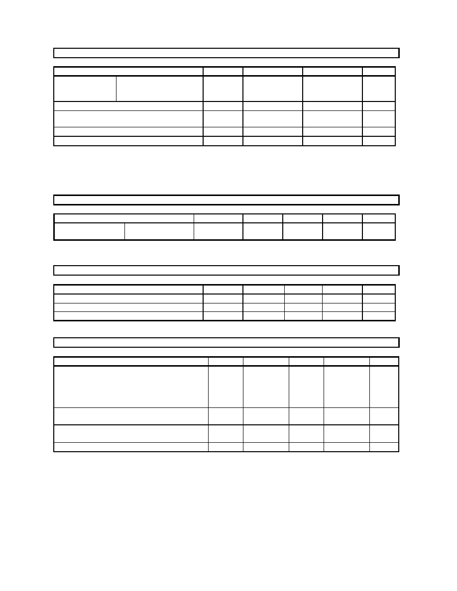
ABSOLUTE MAXIMUM RATINGS
(AVSS, DVSS=0V; Note 2)
Parameter Symbol
min
max
Units
Power Supplies:
Analog
Digital
|AVSS-DVSS| (Note 3)
AVDD
DVDD
GND
-0.3
-0.3
4.6
4.6
0.3
V
V
V
Input Current (Any pins except supplies)
IIN
-
±10
mA
Input Voltage (Except RX0, RX1 pins)
(RX0, RX1 pins)
VIN1
VIN2
-0.3
-0.3
DVDD+0.3
AVDD+0.3
V
V
Ambient Temperature (Power applied)
Ta
-40
85
∞C
Storage Temperature
Tstg
-65
150
∞C
Note 2. All voltages with respect to ground.
Note 3. AVSS and DVSS must be connected to the same ground.
WARNING: Operation at or beyond these limits may result in permanent damage to the device.
Normal operation is not guaranteed at these extremes.
RECOMMENDED OPERATING CONDITIONS
(AVSS, DVSS=0V; Note 2)
Parameter Symbol
min
typ
max
Units
Power Supplies:
Analog
Digital
AVDD
DVDD
2.7
2.7
3.3
3.3
3.6
AVDD
V
V
Note 2. All voltages with respect to ground.
S/PDIF RECEIVER CHARACTERISTICS
(Ta=25
∞C; AVDD, DVDD=2.7~3.6V)
Parameter Symbol
min
typ
max
Units
Input Resistance
Zin
-
10
-
k
Input Voltage
VTH
350
mVpp
Input Sample Frequency
fs
32
-
48
kHz
DC CHARACTERISTICS
(Ta=25∞C; AVDD, DVDD=2.7~3.6V; unless otherwise specified)
Parameter Symbol
min
typ
max
Units
Power Supply Current
Normal operation (PDN= "H") (Note 4)
CM1-0= "00" (Note 5)
CM1-0= "01" (Note 6)
Power down (PDN = "L") (Note 7)
7
2
10
14
-
100
mA
mA
µA
High-Level Input Voltage
Low-Level Input Voltage
VIH
VIL
70%DVDD
DVSS-0.3
-
-
DVDD+0.3
30%DVDD
V
V
High-Level Output Voltage (Iout=-400µA)
Low-Level Output Voltage (Iout=400
µA)
VOH
VOL
DVDD-0.4
-
-
-
-
0.4
V
V
Input Leakage Current
Iin
-
-
± 10
µA
Note 4. AVDD=DVDD=3.3V.
Note 5. fs=48kHz, X'tal=24.576MHz, C
L
=20pF. AVDD=5mA (typ), DVDD=9mA (typ).
Note 6. fs=48kHz, X'tal=24.576MHz. The external load current is not included.
Note 7. RX inputs are open and all digital input pins are held at DVDD or DVSS.