þÿ
AIC1563
Versatile DC/DC Converter
Analog Integrations Corporation 4F, 9 Industry E. 9th Rd, Science-Based Industrial Park, Hsinchu, Taiwan
DS-1563-02 012102
TEL: 886-3-5772500
FAX: 886-3-5772510
www.analog.com.tw
1
n
FEATURES
l
3V to 30V Input Voltage Operation.
l
Internal 2A Peak Current Switch.
l
1.5A Continuous Output Current.
l
Bootstrapped Driver.
l
High Side Current Sense Capability.
l
High Efficiency (up to 90%).
l
Internal
±
2% Reference.
l
Low Quiescent Current at 1.6mA.
l
Frequency Operation from 100Hz to 100KHz.
n
APPLICATIONS
l
Constant Current Source for Battery Chargers.
l
Saver for Cellular phones.
l
Step-Down DC-DC Converter Module.
n
DESCRIPTION
The AIC1563 is a monolithic control circuit con-
taining the primary functions required for DC to
DC converters and highside-sensed constant cur-
rent source. The device consists of an internal
temperature compensated reference, comparator,
controlled duty cycle oscillator with an active cur-
rent sense circuit, bootstrapped driver, and high
current output switch. This device is specifically
designed to construct a constant current source
for battery chargers with a minimum number of
external components. Bootstrapped driver can
drive the NPN output switch to saturation for
higher efficiency and less heat dissipation. The
AIC1563 can deliver 1.5A continuous current
without requiring a heat sink.
n
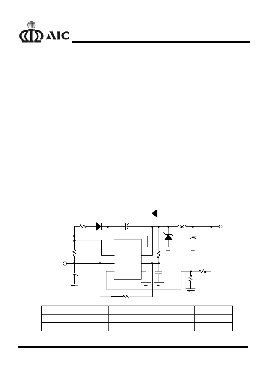
TYPICAL APPLICATION CIRCUIT
+
C3
1
µ
F
470
µ
F
+ C1
100
µ
F
C2
1000pF
R1
470
RB
3K
R3
2.2M
RS
0.22
RA
1K
R2
390K
D1
1N5819
D3
D2
1N4148
L1
300
µ
H
AIC1563
8
7
6
5
4
3
2
1
BOOST
FB
GND
IS
DC
DE
CF
VCC
+
C4
5V/1A
8V~25V
V
IN
When V
IN
>15V,
Then, R1=1K
1N4148
Line Regulation
V
IN
= 10V~20V @ I
O
=1A
40mV
Load Regulation
V
IN
= 15V, @ I
O
=100mA~1A
20mV
Short Circuit Current
V
IN
=15V, @ R
L
= 0.1
1.3A
Step-Down Converter
AIC1563
AIC1563
2
n
ORDERING INFORMATION
PIN CONFIGURATION
DIP-8
SO-8
TOP VIEW
VCC
BOOST
DE
CF
GND
IS
FB
DC
1
3
4
2
8
6
5
7
PACKING TYPE
TR: TAPE & REEL
TB: TUBE
PACKAGING TYPE
N: PLASTIC DIP
S: SMALL OUTLINE
AIC1563-CXXX
Example: AIC1563CSTR
à
in SO-8 Package & Taping & Reel
Packing Type
(CN is not available in TR packing)
n
ABSOLUTE MAXIMUM RATINGS
Supply Voltage................................................................. ... ... ... ... .............................
30V
Comparator Input Voltage Range ............................................... ... ... ... .......... -0.3V~30V
Switch Collector Voltage....................................................... ... ... ... ... ......................... 30V
Switch Emitter Voltage......................................................... ... ... ... ... ......................... 30V
Switch Collector to Emitter Voltage ..................................... ... ... ... ............................. 30V
Driver Collector Voltage....................................................... ... ... ... ... .......................... 30V
Switch Current ................................................... ... ... ... ... ... ......................................... 2A
Power Dissipation and Thermal Characteristics
DIP Package
Ta= 25
°
C............................... ... ... ... ................................ 1.0W
Thermal Resistance ................ ... ... ... ......................... 100
°
C/W
SO Package
Ta= 25
°
C......................... ... ... ... ... ............................... 625mW
Thermal Resistance ...................... ... ... ...................... 160
°
C/W
Operating Junction Temperature ........................................................ ... ... ............. 125
°
C
Operating Ambient Temperature Range .......................... ... ... ... ... ......................... 0~70
°
C
Storage Temperature Range ...................................... ... ... ... .................... - 65
°
C ~ 150
°
C
AIC1563
AIC1563
3
n
TEST CIRCUIT
BOOST
AIC1563
8
7
6
5
4
3
2
1
DC
IS
DE
CF
GND
FB
VCC
R1
1K
CT
1nF
1A
Current Source
VCC
1.275V
VCC
50mA
Current Source
4.55V
@VCC=5V
4.75V
2V/0V
I
DISCHG
/ I
CHG
1.225V
n
ELECTRICAL CHARACTERISTICS
(V
CC
= 5V, T
A
=25
°
C, unless otherwise specified.)
PARAMETER
TEST CONDITIONS
SYMBOL
MIN.
TYP.
MAX.
UNIT
Oscillator
Charging Current
5.0V
VCC
30V
I
CHG
10
25
40
µ
A
Discharge Current
5.0V
VCC
30V
I
DISCHG
100
150
200
µ
A
Voltage Swing
PIN 3
V
OSC
0.6
V
Discharge to Charge Current
Ratio
V
IS
=VCC
I
DISCHG
/
I
CHG
6.0
Current Limit Sense Voltage
I
CHG
=I
DISCHG
VCC V
IS
250
300
350
mV
Output Switch
Saturation Voltage, Emitter
Follower Connection
I
DE
=1.0A;
V
BOOST
=V
DC
= VCC
V
CE(SAT)
1.5
1.8
V
Saturation Voltage
I
DC
=1.0A; I
BOOST
=50mA, (Forced
20)
V
CE (SAT)
0.4
0.7
V
DC Current Gain
I
SC
=1.0A; V
CE
=5.0V
h
FE
35
120
Collector Off-State Current
V
CE
=30V
I
C(OFF)
10
nA
AIC1563
AIC1563
4
n
ELECTRICAL CHARACTERISTICS
(V
CC
= 5V, T
A
=25
°
C, unless otherwise specified.)
PARAMETER
TEST CONDITIONS
SYMBOL
MIN.
TYP.
MAX.
UNIT
Comparactor
Threshold Voltage
T
A
=25
°
C
0
°
C
T
A
70
°
C
V
FB
1.225
1.21
1.25
1.275
1.29
V
V
Threshold Voltage Line
Regulation
3.0V
VCC
30V
REG
LINE
0.1
0.3
mV/V
Input Bias Current
V
IN
=0V
I
IB
0.4
1
µ
A
Supply Current
V
IS
=VCC, pin 5>V
FB
5.0V
VCC
30V
C
T
=1nF
PIN 2=GND
Remaining pins open
I
CC
1.6
3
mA
n
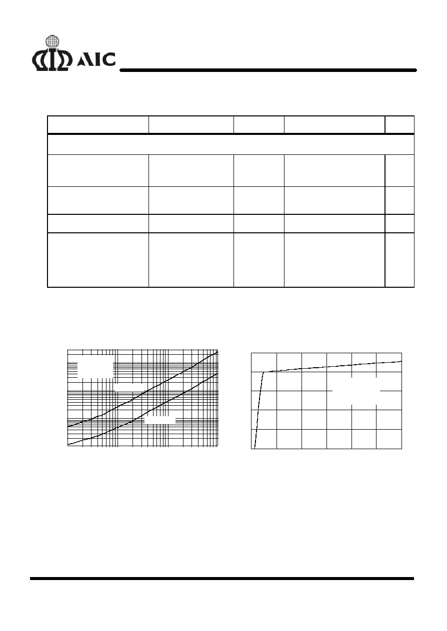
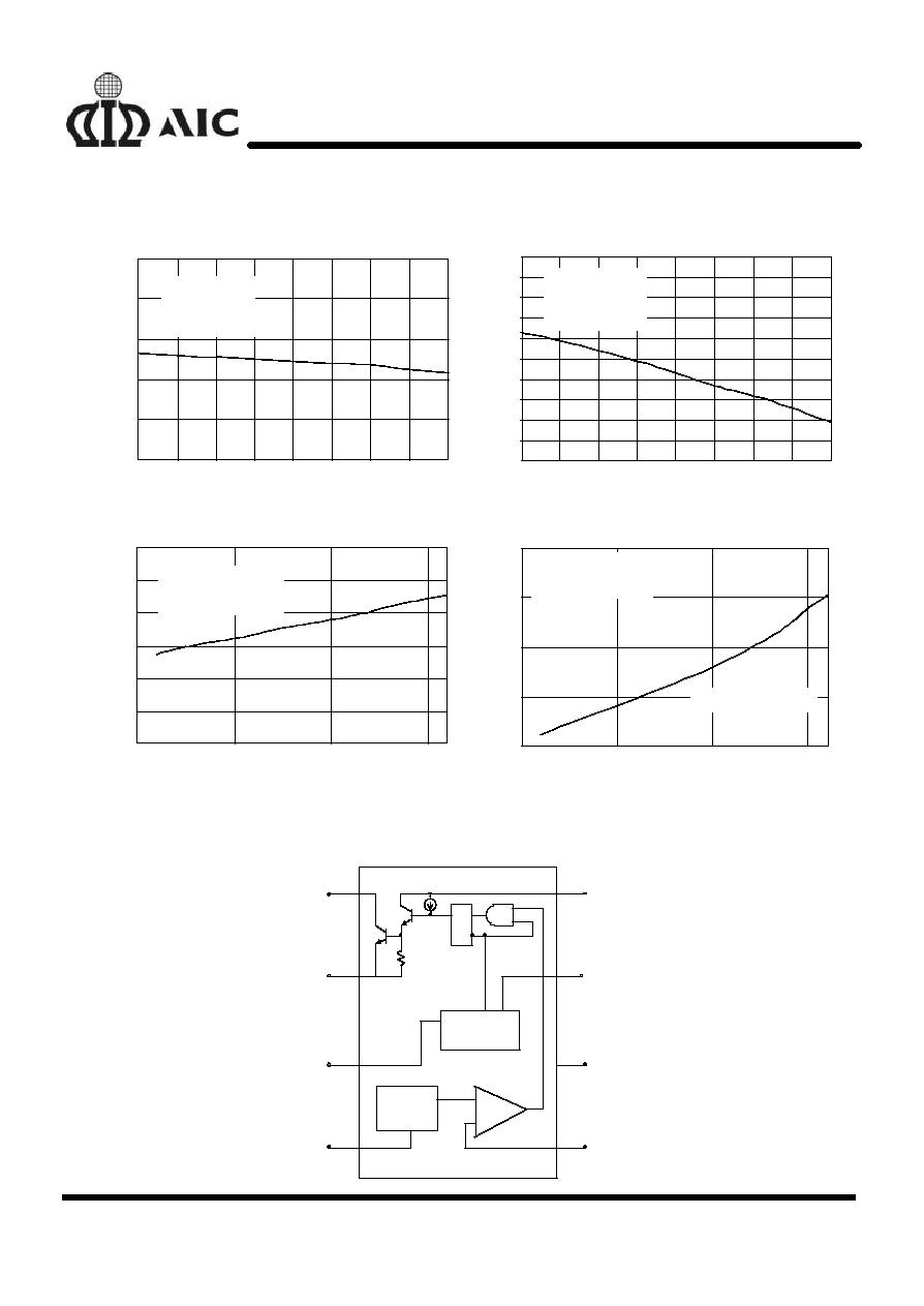
TYPICAL PERFORMANCE CHARACTERISTICS
CT, Oscillator Timing Capacitor (nF)
t
ON
-OFF
, Output Switch ON-OFF Time (
µ
S)
Fig. 1 Output Switch ON-OFF Time vs. Oscillator
Timing Capacitor
0.1
1
10
100
1
10
100
1000
OFF-TIME
ON -TIME
VCC=5V
V
IS
=VCC
PIN 5=GND
Fig. 2 Standby Supply Current vs.
Supply Voltage
VCC, Supply Voltage (V)
I
CC
, Supply Current (mA)
0
5
10
15
20
25
30
0
0.4
0.8
1.2
1.6
2
C
T
= 1nF
V
IS
= VCC
PIN 2 =GND
AIC1563
AIC1563
5
n
TYPICAL PERFORMANCE CHARACTERISTICS
(Continued)
V
FB
, Threshold Voltage (V)
Temperature (
°
C)
Fig. 3 V
FB
, Threshold Voltage vs. Temperature
1.2
1.22
1.24
1.26
1.28
1.3
0
10
20
30
40
50
60
70
80
VCC = 5V,
C
T
= 1nF,
PIN 2 = GND
V
CC
-V
IS
Threshold Voltage (
m
V)
Temperature (
°
C)
Fig. 4 I
S
Threshold Voltage vs. Temperature
250
260
270
280
290
300
0
10
20
30
40
50
60
70
80
VCC = 5V,
C
T
= 1nF,
PIN 2 = GND
310
320
330
340
350
Fig. 5 Emmiter Follower Configuration Output Switch
Saturation Voltage vs. Emmiter Current
I
E
, Emitter Current (A)
1.2
1.3
1.4
1.5
1.6
1.7
1.8
V
CE(SAT)
, Saturation Voltage (V)
0
0.5
1
1.5
VCC = 5V
PIN 1, 7, 8 = VCC
PIN 3, 5 = GND
Fig. 6 Common Emitter Configuration Output Switch
Saturation Voltage vs. Collector Current
I
C
, Collector Current (A)
V
CE(SAT)
, Saturation Voltage (V)
0
0.5
1
1.5
0
0.2
0.4
0.6
0.8
VCC = 5V
PIN 7 = VCC
PIN 2, 3, 5 =
GND
Forced Beta = 20
n
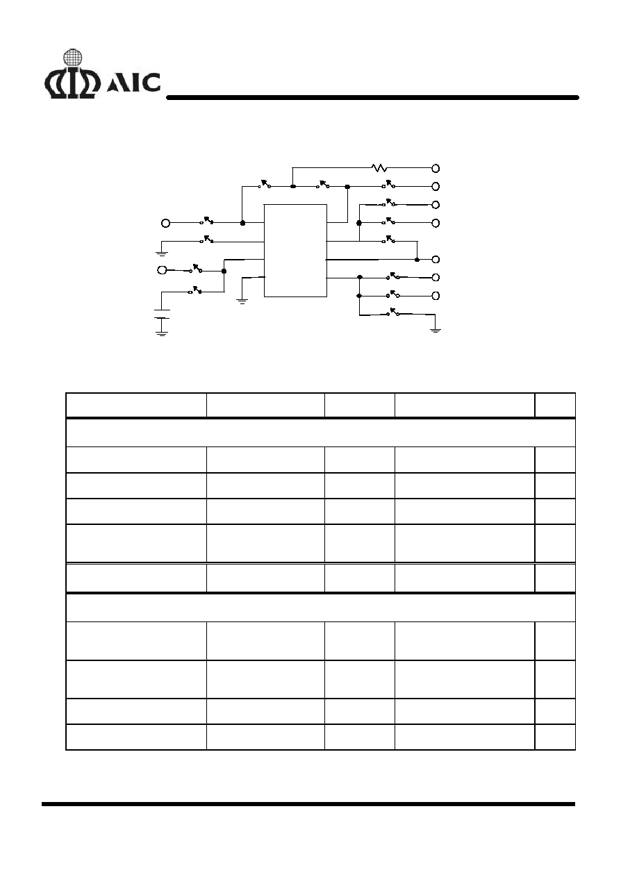
BLOCK DIAGRAM
Q
R
S
BOOST
IS
VCC
FB
GND
CF
DC
DE
8
7
6
5
4
3
2
1
Q1
Oscillator
Is
CT
Comparator
-
+
1.25V
Reference
Voltage
Q2
80
AIC1563
AIC1563
6
n
PIN DESCRIPTIONS
PIN 1: DC
- The switch collector is 2A.
PIN 2: DE
- Darlington switch emitter.
PIN 3: CF
- Oscillator timing capacitor.
PIN 4: GND - Power ground.
PIN 5: FB
- Feedback comparator inverting input.
PIN 6: VCC - Power supply input.
PIN 7: IS
- Highside current sense input.
VCC - V
IS
=300mV.
PIN 8: BOOST -Bootstrapped driver collector.
n
APPLICATION INFORMATIONS
l
DESIGN FORMULA TABLE
CALCULATION
STEP-DOWN
STEP-UP
t
t
ON
OFF
V + V
V
- V - V
OUT
F
IN(MIN)
SAT
OUT
V + V
V
V
- V
OUT
F
IN(MIN)
IN(MIN)
SAT
-
(t
ON
+ t
OFF
)
MAX
1
F
MIN
1
F
MIN
C
T
4x10
-5
t
ON
4 x 10
-5
t
ON
I
C (SWITCH)
2I
OUT(MAX)
2I
OUT(MAX)
(
)
t + t
t
ON
OFF
OFF
RS
0.3/I
C(SWITCH)
0.3/ I
C (SWITCH)
L(MIN)
(
)
V
- V - V
I
t
IN(MIN)
SAT
OUT
C(SWITCH)
ON(MAX)
(
)
V
- V
I
t
IN(MIN)
SAT
C(SWITCH)
ON(MAX)
Co
I
( t + t
8 V
C ( SWITCH)
ON
OFF
RIPPLE (P - P)
)
I t
V
OUT
ON
RIPPLE(P - P)
V
SAT
= Saturation voltage of the output switch.
V
F
= Forward voltage of the ringback rectifier
The following power supply characteristics must be
chosen:
V
IN
-
Nominal input voltage.
V
OUT
-
Desired output voltage,
V
OUT
= 1.25 (1 + RB/RA)
I
OUT
-
Desired output current.
F
MIN
-
Minimum desired switching frequency at
selected values for V
IN
and I
OUT
.
V
RIPPLE (P-P)
-
Desired peak-to-peak output ripple volt-
age. In practice, the calculated value will
need to be increased due to the capacitor
equivalent series resistance and board
layout. The ripple voltage should be kept to
a low value since it will directly affect the
line and load regulation.
AIC1563
AIC1563
6
n
APPLICATION EXAMPLES
PEAK
1
VBT
2
DIS
3
VTS
4
VCC
5
ADJ
6
SEL3
7
TMR
8
MODE
9
SEL2
10
SEL1
11
GND
12
LED1
13
LED2 14
ICON
15
DSW 16
U2
AIC1781
R8
300K
R9
91K
R10
100K
+
C9
4.7
µ
F
C7
0.1
µ
F
C10
47nF
R15
680
R3
270
R2
20/5W
SW1
PB SW
R12
100K
R16
680
R17
680
R14
200K
C8
0.
1
µ
F
+
C11
100
µ
F
RX
R11
100K
RY
C6
0.1
µ
F
R13
470K
Q2
MMBT2222A
R6
50K
LED2
GREEN
LED3
RED
LED1
YELLOW
Q1
MPS2222A
+
C4
220
µ
F
C5
0
.1
µ
F
+
C12
1
µ
F
+
C13
10
µ
F
R5 120/0.5W
R1
1K
BAT1
**
BATTERY
R7
THERMISTOR
VIN
11~15V
L1
220
µ
H
C2
1
µ
F
C1
470P
RS
0.3/1W
1
2
3
GND
4
FB
5
VCC
DC
DE
CF
6
IS
7
BOOST
8
U1
AIC1563
+
C3
220
µ
F
R4
390K
D3
IN4148
D1
IN4148
D2 IN5819
D4
1N5819
VIN
VOUT
GND
U3
78L05
**3~5 NiMH/NiCd cells.
Note: Charge Current=0.3/RS Ampere
Safety Timer: 80min
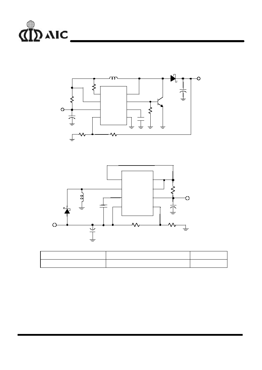
Fig. 1 Battery Charge Circuit for Fluctuating Charging Current Applications
BOOST
IS
DC
DE
CF
GND
*RS
V
IN
L
220
µ
H
D2
1N4148
RB
33K
D3
1N5819
1K
C
O
C1
D 1
1N5821
C3
1
µ
F
CT
470pF
R A
5.6K
220
µ
F
+
+
AIC1563
C 5
10
µ
F
+
R1
*I
O
=300mV/RS
I
O
R2
120
220
µ
F
VCC
FB
(%)
Io (A )
0
0.5
1
1.5
2
70
80
90
100
V
IN
= 16 V, V
O
= 8 V
V
IN
= 16 V, V
O
= 1 2 V
Efficiency vs Output Current
Fig. 2 Battery Charge Circuit
AIC1563
AIC1563
7
n
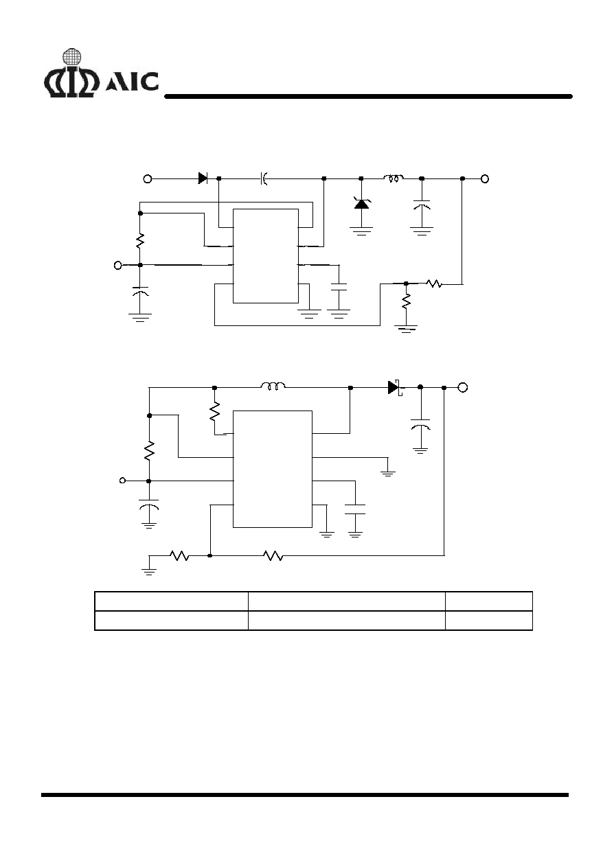
APPLICATION EXAMPLES
(Continued)
16V~25V
+
C3
1
µ
F
C4
470
µ
F
+
C1
100
µ
F
C2
470pF
RB
13K
RA
1K
RS
0.22
D1
1N5819
D1
1N5819
L1
300
µ
H
AIC1563
8
7
6
5
4
3
2
1
BOOST
FB
GND
IS
DC
DE
CF
VCC
+
5V
12V/1A
V
IN
Fig. 3 Step-Down Converter with External 5V Bootstrap
D1
BOOST
AIC1563
IS
8
7
6
5
4
3
2
1
FB
VCC
L1
200
µ
H
RB
47K
RA
2K2
C1
C0
CT
680pF
RS
0.22
V
OUT
V
IN
28V/200mA
1N5819
100
µ
F
220
µ
F
+
+
R1
150
DC
DE
GND
CF
8~16V
Line Regulation
V
IN
= 8V~16V @ I
O
=200mA
100mV
Load Regulation
V
IN
= 12V, @ I
O
=80mA~200mA
40mV
Fig. 4 Step-Up Converter
AIC1563
AIC1563
8
n
APPLICATION EXAMPLES
(Continued)
BOOST
AIC1563
IS
8
7
6
5
4
3
2
1
FB
VCC
DC
DE
CF
GND
V
OUT
V
IN
+
+
C
0
D1
Q1
R2
CT
RB
C1
RS
R1
L
RA
Fig. 5 Step-Up Converter with External NPN Switch
D1
1N5819
100
µ
H
RA
8.2K
953
RB
C1
C
0
CT
RS
0.26
AIC1563
8
7
6
5
4
3
2
1
CF
GND
100
µ
F
V
OUT
-12V/100mA
V
IN
4.5V~6V
560pF
470
µ
F
+
+
L1
DC
DE
VCC
FB
BOOST
IS
Line Regulation
V
IN
= 4.5V~6V @ I
O
=100mA
20mV
Load Regulation
V
IN
= 5V, @ I
O
=10mA~100mA
100mV
Fig. 6 Inverting Converter
AIC1563
AIC1563
9
n
PHYSICAL DIMENSIONS
l
8 LEAD PLASTIC SO (unit: mm)
SYMBOL
MIN
MAX
A
1.35
1.75
A1
0.10
0.25
B
0.33
0.51
C
0.19
0.25
D
4.80
5.00
E
3.80
4.00
e
1.27(TYP)
H
5.80
6.20
L
0.40
1.27
D
H
e
A
B
A1
C
E
L
l
8 LEAD PLASTIC DIP (unit: mm)
SYMBOL
MIN
MAX
A1
0.381
--
A2
2.92
4.96
b
0.35
0.56
C
0.20
0.36
D
9.01
10.16
E
7.62
8.26
E1
6.09
7.12
e
2.54 (TYP)
eB
--
10.92
b
e
L
A2
A1
eB
E
C
E1
D
L
2.92
3.81