 | ÐлекÑÑоннÑй компоненÑ: AD684A | СкаÑаÑÑ:  PDF PDF  ZIP ZIP |
AD684* Four-Channel Sample-and-Hold Amplifier
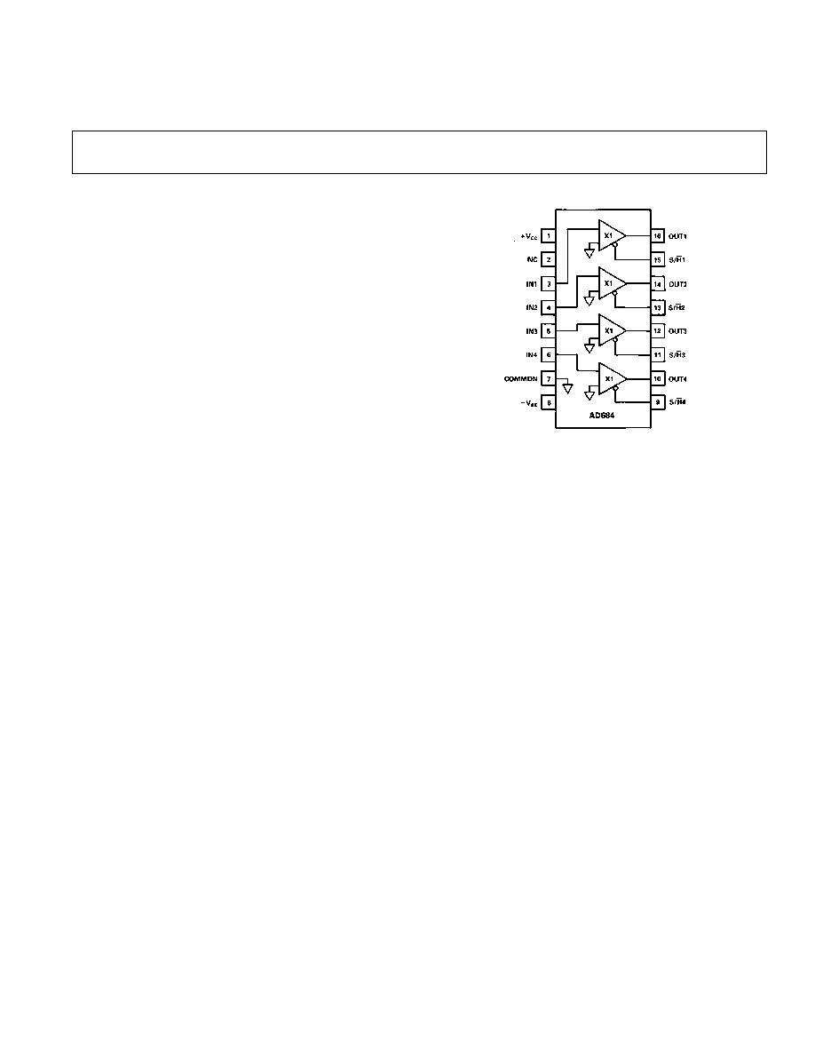
FUNCTIONAL BLOCK DIAGRAM
REV. A
Information furnished by Analog Devices is believed to be accurate and
reliable. However, no responsibility is assumed by Analog Devices for its
use, nor for any infringements of patents or other rights of third parties
which may result from its use. No license is granted by implication or
otherwise under any patent or patent rights of Analog Devices.
a
Four-Channel
Sample-and-Hold Amplifier
AD684*
One Technology Way, P.O. Box 9106, Norwood, MA 02062-9106, U.S.A.
Tel: 617/329-4700
Fax: 617/326-8703
FEATURES
Four Matched Sample-and-Hold Amplifiers
Independent Inputs, Outputs and Control Pins
500 ns Hold Mode Settling
1
s Maximum Acquisition Time to 0.01%
Low Droop Rate: 0.01
V/ s
Internal Hold Capacitors
75 ps Maximum Aperture Jitter
Low Power Dissipation: 430 mW
0.3" Skinny DIP Package
MIL-STD-883 Compliant Versions Available
PRODUCT HIGHLIGHTS
1. Fast acquisition time (1
µ
s) and low aperture jitter (75 ps)
make the AD684 the best choice for multiple channel data
acquisition systems.
2. Monolithic construction insures excellent interchannel
matching in terms of timing and accuracy, as well as high
reliability.
3. Independent inputs, outputs and sample-and-hold controls
allow user flexibility in system architecture.
4. Low droop (0.01
µ
V/
µ
s) and internally compensated hold
mode error results in superior system accuracy.
5. The AD684's fast settling time and low output impedance
make it ideal for driving high speed analog to digital
converters such as the AD578, AD674, AD7572 and the
AD7672.
6. The AD684 is available in versions compliant with MIL-
STD-883. Refer to the Analog Devices Military Products
Databook or current AD684/883B data sheet for detailed
specifications.
PRODUCT DESCRIPTION
The AD684 is a monolithic quad sample-and-hold amplifier
(SHA). It features four complete sampling channels, each
controlled by an independent hold command. Each SHA is
complete with an internal hold capacitor. The high accuracy
SHA channels are self-contained and require no external
components or adjustments. The AD684 is manufactured on a
BiMOS process which provides a merger of high performance
bipolar circuitry and low power CMOS logic.
The AD684 is ideal for high performance, multichannel data
acquisition systems. Each SHA channel can acquire a signal in
less than 1
µ
s and retain the held value with a droop rate of less
than 0.01
µ
V/
µ
s. Excellent linearity and ac performance make
the AD684 an ideal front end for high speed 12- and 14-bit
ADCs.
The AD684 has a self-correcting architecture that minimizes
hold mode errors and insures accuracy over temperature. Each
channel of the AD684 is capable of sourcing 5 mA and
incorporates output short circuit protection.
The AD684 is specified for three temperature ranges. The J
grade device is specified for operation from 0 to +70
°
C, the A
grade from 40
°
C to +85
°
C and the S grade from 55
°
C to
+125
°
C.
*Protected by U.S. Patent Number 4,962,325.
AD684SPECIFICATIONS
(T
MIN
to T
MAX
with V
CC
= +12 V 10%, V
EE
= 12 V 10%, unless otherwise noted)
AD684J
AD684A
AD684S
Parameter
Min
Typ
Max
Min
Typ
Max
Min
Typ
Max
Units
SAMPLING CHARACTERISTICS
Acquisition Time
10 V Step to 0.01%
0.75
1.0
0.75
1.0
0.75
1.0
µ
s
10 V Step to 0.1%
0.5
0.6
0.5
0.6
0.5
0.6
µ
s
Small Signal Bandwidth
4
4
4
MHz
Full Power Bandwidth
1
1
1
MHz
HOLD CHARACTERISTICS
Effective Aperture Delay
35
25
15
35
25
15
35
25
15
ns
Aperture Jitter
50
75
50
75
50
75
ps
Hold Settling Time (to 1 mV)
250
500
250
500
250
500
ns
Droop Rate
l
0.01
1
0.01
1
0.01
1
µ
V/
µ
s
Feedthrough
(V
IN
=
±
5 V, 100 kHz)
90
90
90
dB
ACCURACY CHARACTERISTICS
1
Hold Mode Offset
4
1
+3
4
1
+3
4
1
+3
mV
Hold Mode Offset Drift
10
10
10
µ
V/
°
C
Sample Mode Offset
50
200
50
200
50
200
mV
Nonlinearity
±
0.002
±
0.003
±
0.002
±
0.003
±
0.003
±
0.005
% FS
Gain Error
±
0.03
0.05
±
0.03
0.05
±
0.03
0.05
% FS
INTERCHANNEL CHARACTERISTICS
Interchannel Isolation
(V
IN
=
±
5 V, 100 kHz)
80
86
80
86
80
86
dB
Interchannel Aperture Offset
150
300
150
300
150
300
ps
Interchannel Offset
0.4
1.5
0.4
2.0
0.4
2.0
mV
OUTPUT CHARACTERISTICS
Output Drive Current
2
5
+5
5
+5
5
+5
mA
Output Resistance, dc
0.3
0.5
0.3
0.5
0.3
0.5
Total Output Noise
(dc to 5 MHz)
150
150
150
µ
V rms
Sampled dc Uncertainty
85
85
85
µ
V rms
Hold Mode Noise
(dc to 5 MHz)
125
125
125
µ
V rms
Short Circuit Current
3
Source
20
20
20
mA
Sink
10
10
10
mA
INPUT CHARACTERISTICS
Input Voltage Range
5
+5
5
+5
5
+5
V
Bias Current
4
100
250
100
250
100
250
nA
400
500
500
nA
Input Impedance
50
50
50
M
Input Capacitance
2
2
2
pF
DIGITAL CHARACTERISTICS
Input Voltage Low
0.8
0.8
0.8
V
Input Voltage High
2.0
2.0
2.0
V
Input Current (V
IN
= 5 V)
2
10
2
10
2
10
µ
A
POWER SUPPLY CHARACTERISTICS
Operating Voltage Range (V
CC
, V
EE
)
±
10.8
±
12
±
13.2
±
10.8
±
12
±
13.2
±
10.8
±
12
±
13.2
V
Supply Current
18
25
18
25
18
26
mA
+PSRR
65
70
65
70
65
70
dB
PSRR
60
65
60
65
60
65
dB
Power Consumption
430
600
430
600
430
625
mW
TEMPERATURE RANGE
Specified Performance
0
+70
40
+85
55
+125
°
C
PACKAGE OPTIONS
16-Pin Cerdip (Q)
AD684JQ
AD684AQ
AD684SQ
NOTES
1
Specified and tested over an input range of
±
5 V.
2
Maximum current the AD684 can source (or sink). Testing guarantees that the accuracy of the held signal remains within 2.5 mV of its initial value.
3
The output is protected for a short circuit to common, V
CC
and V
EE
.
4
V
CC
and V
EE
at nominal voltage levels.
Specifications shown in boldface are tested on all production units at final electrical test. Results from those tests are used to calculate outgoing quality levels. All min and max
specifications are guaranteed, although only those shown in boldface are tested on all production units.
Specifications subject to change without notice.
REV. A
2
AD684
REV. A
3
ABSOLUTE MAXIMUM RATINGS*
With
Spec
Respect to
Min
Max
Unit
V
CC
Common
0.3
+15
V
V
EE
Common
15
+0.3
V
Control Inputs
Common
0.5
+7
V
Analog Inputs
Common
12
+12
V
Output Short Circuit to
Ground, V
CC
or V
EE
Indefinite
Max Junction
Temperature
+175
°
C
Storage
65
+150
°
C
Lead Temperature
(10 sec max)
+300
°
C
Power Dissipation
640
mW
*Stresses above those listed under "Absolute Maximum Ratings" may cause
permanent damage to the device. This is a stress rating only and functional
operation of the device at these or any other conditions above those indicated in the
operational section of this specification is not implied.
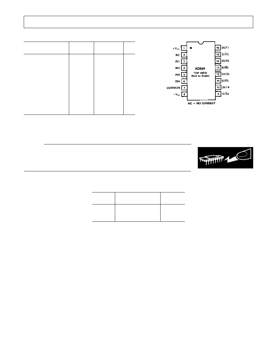
PIN CONFIGURATION
WARNING!
ESD SENSITIVE DEVICE
CAUTION
ESD (electrostatic discharge) sensitive device. Electrostatic charges as high as 4000 V readily
accumulate on the human body and test equipment and can discharge without detection.
Although the AD684 features proprietary ESD protection circuitry, permanent damage may
occur on devices subjected to high energy electrostatic discharges. Therefore, proper ESD
precautions are recommended to avoid performance degradation or loss of functionality.
ORDERING GUIDE
Package
Model
1
Temperature Range
Option
2
AD684JQ
0 to +70
°
C
Q-16
AD684AQ
40
°
C to +85
°
C
Q-16
AD684SQ
55
°
C to +125
°
C
Q-16
NOTES
1
For details on grade and package offerings screened in accordance
with MIL-STD-883, refer to the Analog Devices Military Prod-
ucts Databook or current AD684/883B data sheet.
2
Q = Cerdip.
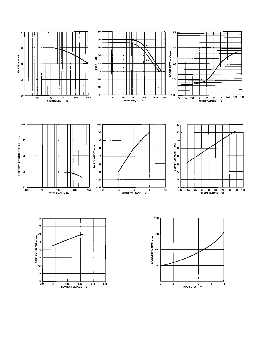
AD684Typical Characteristics
REV. A
4
Droop Rate vs. Temperature, V
IN
= 0 V
Effective Aperture Delay vs. Frequency
Bias Current vs. Input Voltage
Supply Current vs. Temperature
Supply Current vs. Supply Voltage
Interchannel Isolation vs. Frequency
Power Supply Rejection Ratio
vs. Frequency
Acquisition Time (to 0.01 %) vs. Input Step Size
AD684
REV. A
5
DEFINITIONS OF SPECIFICATIONS
Acquisition Time
-- The length of time that the SHA must
remain in the sample mode in order to acquire a full-scale input
step to a given level of accuracy.
Small Signal Bandwidth
-- The frequency at which the held
output amplitude is 3 dB below the input amplitude, under an
input condition of a 100 mV p-p sine wave.
Full Power Bandwidth
-- The frequency at which the held
output amplitude is 3 dB below the input amplitude, under an
input condition of a 10 V p-p sine wave.
Effective Aperture Delay
-- The difference between the
switch delay and the analog delay of the SHA channel. A
negative number indicates that the analog portion of the overall
delay is greater than the switch portion. This effective delay
represents the point in time, relative to the hold command, that
the input signal will be sampled.
Aperture Jitter
-- The variations in aperture delay for
successive samples. Aperture jitter puts an upper limit on the
maximum frequency that can be accurately sampled.
Hold Settling Time
--The time required for the output to
settle to within a specified level of accuracy of its final held
value after the hold command has been given.
Droop Rate
-- The drift in output voltage while in the hold
mode.
Feedthrough
-- The attenuated version of a changing input
signal that appears at the output when the SHA is in the hold
mode.
Hold Mode Offset
-- The difference between the input signal
and the held output. This offset term applies only in the hold
mode and includes the error caused by charge injection and all
other internal offsets. It is specified for an input of 0 V.
Tracking Mode Offset
-- The difference between the input
and output signals when the SHA is in the track mode.
Nonlinearity
-- The deviation from a straight line on a plot of
input vs. (held) output as referenced to a straight line drawn
between endpoints, over an input range of 5 V and +5 V.
Gain Error
-- Deviation from a gain of +1 on the transfer
function of input vs. held output.
Interchannel Isolation
-- The level of crosstalk between
adjacent channels while in the sample (track) mode with a full
scale 100 kHz input signal.
Interchannel Aperture Offset
-- The variation in aperture
time between the four channels for a simultaneous hold
command.
Differential Offset
-- The difference in hold mode offset
between the four SHA channels.
Power Supply Rejection Ratio
-- A measure of change in the
held output voltage for a specified change in the positive or
negative supply.
Sampled dc Uncertainty
-- The internal rms SHA noise that
is sampled onto the hold capacitor.
Hold Mode Noise
-- The rms noise at the output of the SHA
while in the hold mode, specified over a given bandwidth.
Total Output Noise
-- The total rms noise that is seen at the
output of the SHA while in the hold mode. It is the rms
summation of the sampled dc uncertainty and the hold mode
noise.
Output Drive Current
-- The maximum current the SHA can
source (or sink) while maintaining a change in hold mode offset
of less than 2.5 mV.
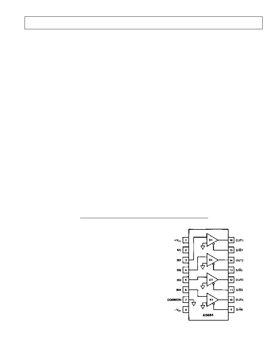
FUNCTIONAL DESCRIPTION
The AD684 is a complete quad sample-and-hold amplifier that
provides high speed sampling to 12-bit accuracy in less than 1
µ
s.
The AD684 is completely self-contained, including on-chip
hold capacitors, and requires no external components or
adjustments to perform the sampling function. Each SHA
channel can operate independently, having its own input, output
and sample/hold command. Both inputs and outputs are treated
as single ended signals, referred to common.
The AD684 utilizes a proprietary circuit design which includes a
self-correcting architecture. This sample-and-hold circuit
corrects for internal errors after the hold command has been
given, by compensating for amplifier gain and offset errors, and
charge injection errors. Due to the nature of the design, the
SHA output in the sample mode is not intended to provide an
accurate representation of the input. However, in hold mode,
the internal circuitry is reconfigured to produce an accurately
held version of the input signal. To the right is a block diagram
of the AD684.
Functional Block Diagram
AD684
REV. A
6
OP484
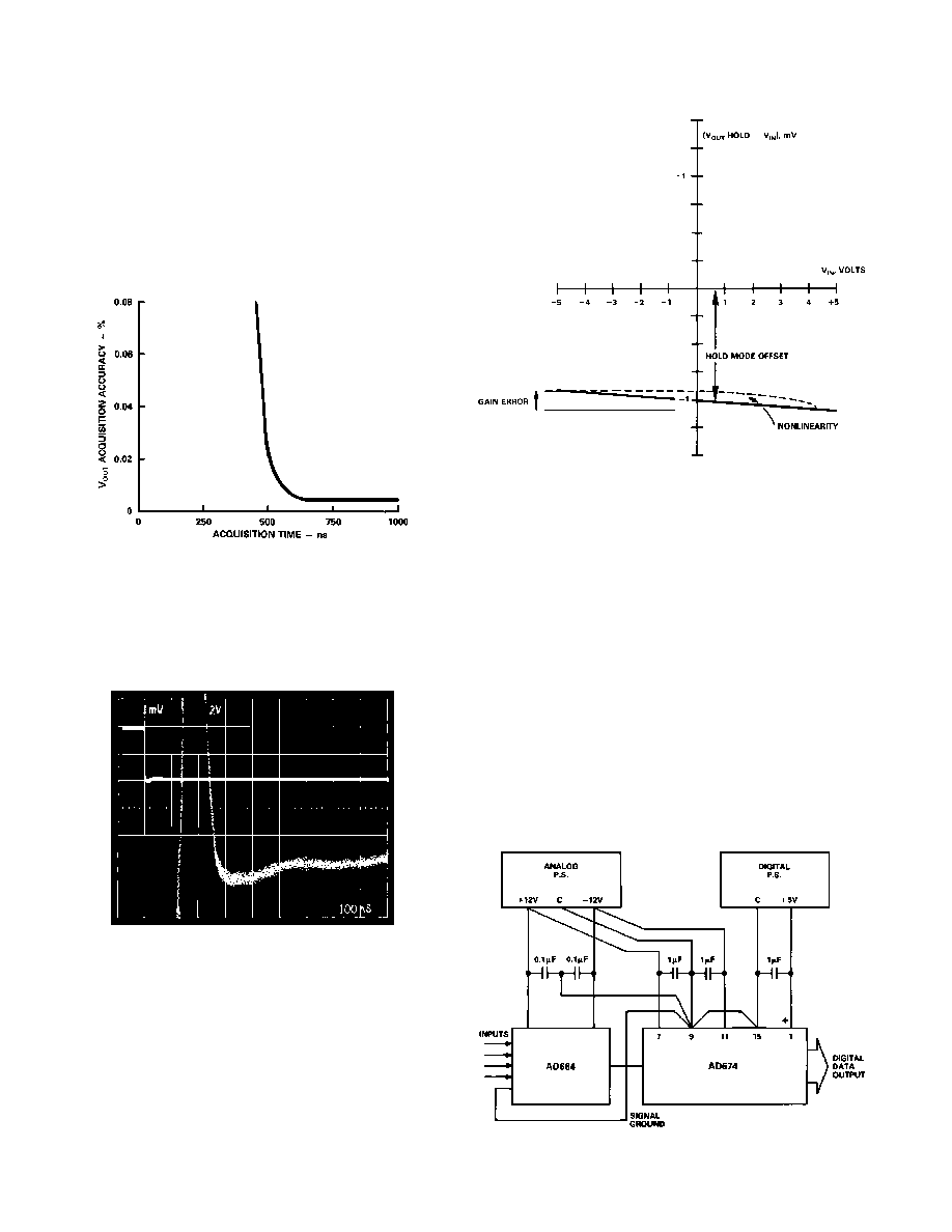
DYNAMIC PERFORMANCE
The AD684 is compatible with 12-bit A-to-D converters in
terms of both accuracy and speed. The fast acquisition time, fast
hold settling time and good output drive capability allow the
AD684 to be used with high speed, high resolution A-to-D
converters like the AD674 and AD7672. The AD684's fast
acquisition time provides high throughput rates for multichannel
data acquisition systems. Typically, the sample and hold can
acquire a 10 V step in less than 750 ns. Figure 1 shows the
settling accuracy as a function of acquisition time.
Figure 1. V
OUT
Settling vs. Acquisition Time
The hold settling determines the required time, after the hold
command is given, for the output to settle to its final specified
accuracy. The typical settling behavior of the AD684 is shown
in Figure 2. The settling time of the AD684 is sufficiently fast to
allow the SHA, in most cases, to directly drive an A-to-D
converter without the need for an added "start convert" delay.
Figure 2. Typical AD684 Hold Mode
HOLD MODE OFFSET
The dc accuracy of the AD684 is determined primarily by the
hold mode offset. The hold mode offset refers to the difference
between the final held output voltage and the input signal at the
time the hold command is given. The hold mode offset arises from
a voltage error introduced onto the hold capacitor by charge injec-
tion of the internal switches. The nominal hold mode offset is
specified for a 0 V input condition. Over the input range of
5 V to +5 V, the AD684 is also characterized for an effective gain
error and nonlinearity of the held value, as shown in Figure 3.
As indicated by the AD684 specifications, the hold mode offset is
very well matched between channels and stable over temperature.
Figure 3. Hold Mode Offset, Gain Error and Nonlinearity
For applications where it is important to obtain zero offset, the
hold mode offset may be nulled externally at the input to the
A-to-D converter. Adjustment of the offset may be accom-
plished through the A-to-D itself or by an external amplifier
with offset nulling capability (e.g., AD711). Only a single
adjustment of the offset is necessary for the four SHA channels as a
result of the excellent matching among them. The offset will
change less than 0.5 mV over the specified temperature range.
SUPPLY DECOUPLING AND GROUNDING
CONSIDERATIONS
As with any high speed, high resolution data acquisition system,
the power supplies should be well regulated and free from
excessive high frequency noise (ripple). The supply connection
to the AD684 should also be capable of delivering transient
currents to the device. To achieve the specified accuracy and
dynamic performance, decoupling capacitors must be placed
directly at both the positive and negative supply pins to common.
Ceramic type 0.1
µ
F capacitors should be connected from V
CC
and V
EE
to common.
Figure 4. Basic Grounding and Decoupling Diagram
AD684
REV. A
7
The AD684 does not provide separate analog and digital ground
leads as is the case with most A-to-D converters. The common
pin is the single ground terminal for the device. It is the refer-
ence point for the sampled input voltage and the held output
voltage and also the digital ground return path. The common
pin should be connected to the reference (analog) ground of the
A-to-D converter with a separate ground lead. Since the analog
and digital grounds in the 684 are connected internally, the
common pin should also be connected to the digital ground,
which is usually tied to analog common at the A-to-D converter.
Figure 4 illustrates the recommended decoupling and grounding
practice.
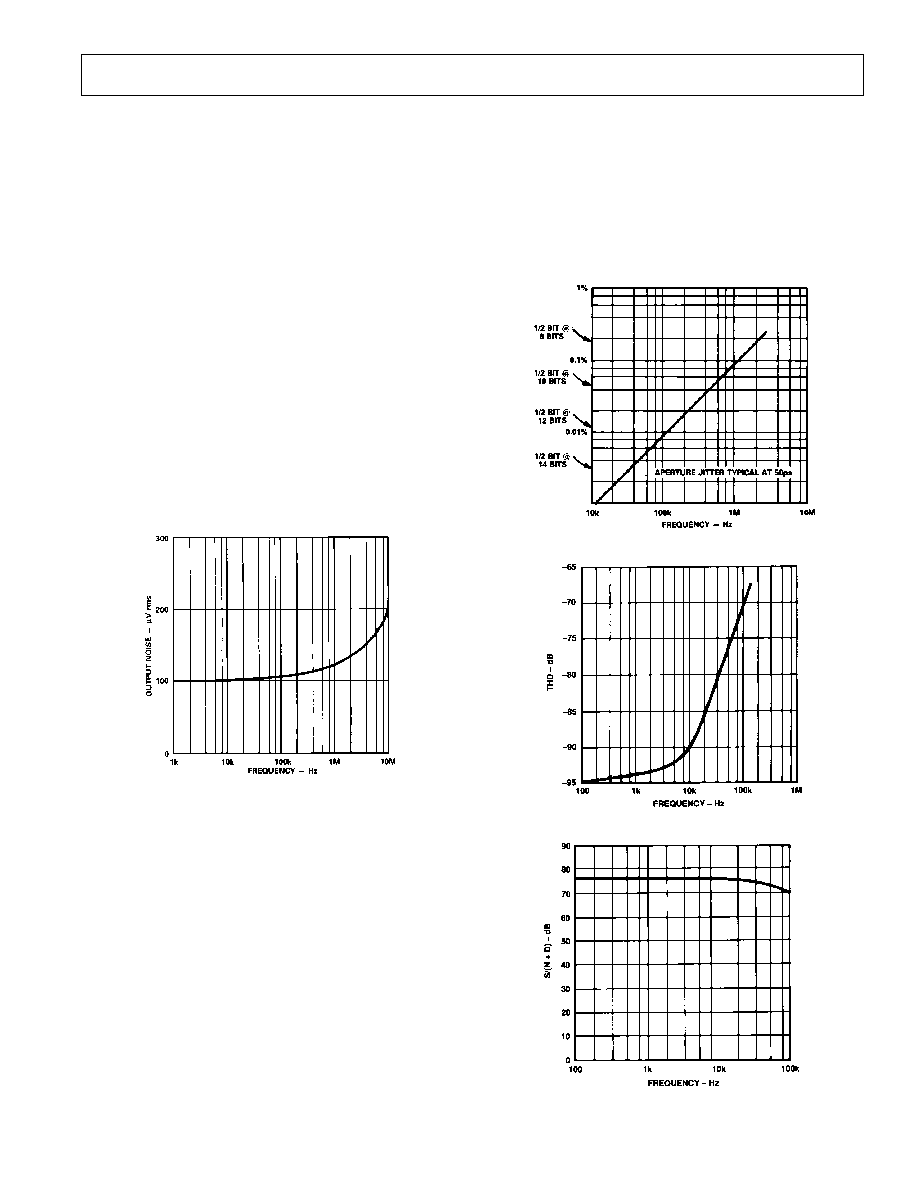
NOISE CHARACTERISTICS
Designers of data conversion circuits must also consider the
effect of noise sources on the accuracy for the data acquisition
system. A sample-and-hold amplifier that precedes the A-to-D
converter introduces some noise and represents another source
of uncertainty in the conversion process. The noise from the
AD684 is specified as the total output noise, which includes
both the sampled wideband noise of the SHA in addition to the
band limited output noise. The total output noise is the rms
sum of the sampled dc uncertainty and the hold mode noise. A
plot of the total output noise vs. the equivalent input bandwidth
of the converter being used is given in Figure 5.
Figure 5. RMS Noise vs. Input Bandwidth of ADC
DRIVING THE ANALOG INPUTS
For best performance, it is important to drive the AD684 analog
inputs from a low impedance signal source. This enhances the
sampling accuracy by minimizing the analog and digital
crosstalk. Signals which come from higher impedance sources
(e.g., over 5k ohms) will have a relatively higher level of
crosstalk. For applications where signals have high source
impedance, an operational amplifier buffer in front of the
AD684 is required. The AD713 (precision quad BiFET op
amp) is recommended for these applications.
HIGH FREQUENCY SAMPLING
Aperture jitter and distortion are the primary factors which limit
frequency domain performance of a sample-and-hold amplifier.
Aperture jitter modulates the phase of the hold command and
produces an effective noise on the sampled analog input. The
magnitude of the jitter induced noise is directly related to the
frequency of the input signal.
A graph showing the magnitude of the jitter induced error vs.
frequency of the input signal is given in Figure 6.
The accuracy in sampling high frequency signals is also con-
strained by the distortion and noise created by the sample-and-
hold. The level of distortion increases with frequency and
reduces the "effective number of bits" of the conversion.
Measurements of Figures 7 and 8 were made using a 14-bit
A-to-D converter with V
IN
= 10 V p-p and a sample frequency
of 100 kSPS.
Figure 6. Error Magnitude vs. Frequency
Figure 7. Total Harmonic Distortion vs. Frequency
Figure 8. Signal/(Noise and Distortion) vs. Frequency
AD684
REV. A
8
C1239a108/91
PRINTED IN U.S.A.
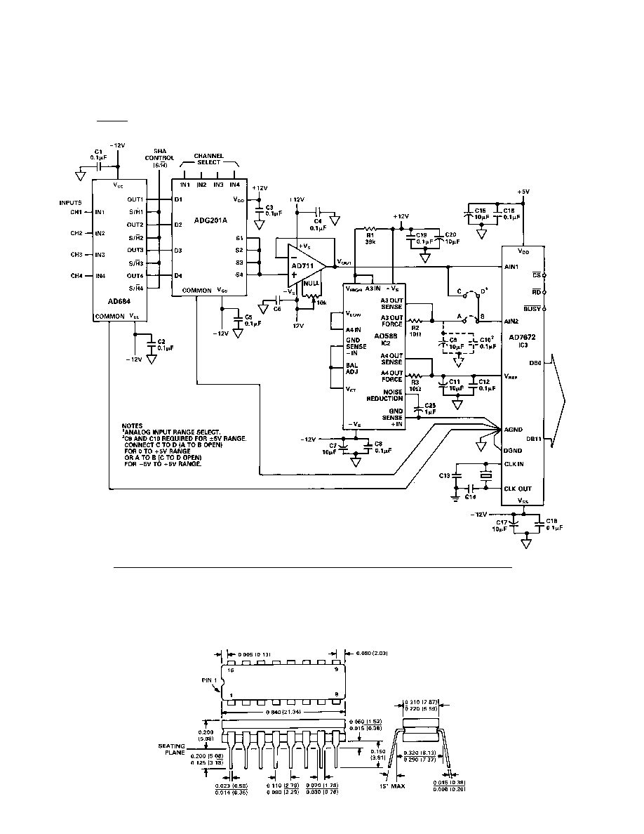
DATA ACQUISITION APPLICATIONS
Figure 9 shows a typical data acquisition circuit using the
AD684 and the high speed 12-bit A-to-D converter, the
AD7672. Four input signals are simultaneously sampled by the
AD684 as the HOLD command is given. One of the four held
outputs is selected by the ADG201, quad CMOS switch, and
buffered by the AD711. The AD588 provides the reference
voltage with switches A-B and C-D selecting a 5 V to +5 V or
0 to +5 V input range.
Figure 9. Data Acquisition System Using the AD684 and the AD7672
OUTLINE DIMENSIONS
Dimensions shown in inches and (mm).
Q-16
16-Lead Cerdip