 | ÐлекÑÑоннÑй компоненÑ: AD5664 | СкаÑаÑÑ:  PDF PDF  ZIP ZIP |
AD5664 2.7 V to 5.5 V, 500 µA, Rail-to-Rail Output Quad 16-Bit nanoDACTM in 10-Lead MSOP Preliminary Data Sheet (Rev. PrA)
2.7 V to 5.5 V, 500 µA, Rail-to-Rail Output
Quad 16-Bit nanoDAC
TM
in 10-Lead MSOP
Preliminary Technical Data
AD5664
Rev. PrA
Information furnished by Analog Devices is believed to be accurate and reliable.
However, no responsibility is assumed by Analog Devices for its use, nor for any
infringements of patents or other rights of third parties that may result from its use.
Specifications subject to change without notice. No license is granted by implication
or otherwise under any patent or patent rights of Analog Devices. Trademarks and
registered trademarks are the property of their respective owners.
One Technology Way, P.O. Box 9106, Norwood, MA 02062-9106, U.S.A.
Tel: 7101.329.4700
www.analog.com
Fax: 7101.326.10703
© 2005 Analog Devices, Inc. All rights reserved.
FEATURES
Low power quad 16-bit nanoDAC
10-lead MSOP and 3mmx3mm LFCSP package
Power-down to 480 nA @ 5 V, 100 nA @ 3 V
2.7 V to 5.5 V power supply
Guaranteed 16-bit monotonic by design
3 power-down functions
Serial interface with Schmitt-triggered inputs
Rail-to-rail operation
SYNC interrupt facility
APPLICATIONS
Process control
Data acquisition systems
Portable battery-powered instruments
Digital gain and offset adjustment
Programmable voltage and current sources
Programmable attenuators
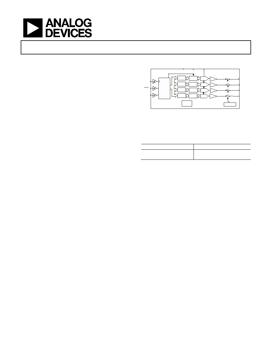
FUNCTIONAL BLOCK DIAGRAM
POWER-
ON
RESET
INTERFACE
LOGIC
DIN
SYNC
SCLK
I
NPUT
REGISTER
I
NPUT
REGISTER
I
NPUT
REGISTER
I
NPUT
REGISTER
D
AC
REGISTER
DAC
REGISTER
DAC
REGISTER
DAC
REGISTER
STRING
DAC C
STRING
DAC A
STRING
DAC B
STRING
DAC D
BUFFER
BUFFER
BUFFER
BUFFER
POWER-DOWN
LO GIC
VOUTB
VOUTC
VOUTD
VDD
VOUTA
V
REF
AD5664
GND
Figure 1.
RELATED DEVICES
Part No.
Description
AD5624R/AD5644R/AD5664R
3 V/5 V 12-/14-/16-bit DAC with
internal reference
GENERAL DESCRIPTION
The AD5664, a member of the nanoDAC family is a low power,
quad, 16-bit buffered voltage-out DAC that operates from a
single 2.7 V to 5.5 V supply and is guaranteed monotonic by
design.
The AD5664 requires an external reference voltage to set the
output range of the DAC. The part incorporates a power-on
reset circuit that ensures the DAC output powers up to 0 V and
remains there until a valid write takes place. The part contains a
power-down feature that reduces the current consumption of
the device to 480 nA at 5 V and provides software-selectable
output loads while in power-down mode.
The low power consumption of this part in normal operation
makes it ideally suited to portable battery-operated equipment.
The power consumption is 3 mW at 5 V, going down to 2.4 µW
in power-down mode.
The AD5664's on-chip precision output amplifier allows rail-to-
rail output swing to be achieved.
The AD5664 uses a versatile 3-wire serial interface that operates
at clock rates up to 50 MHz, and is compatible with standard
SPI®, QSPITM, MICROWIRETM, and DSP interface standards.
PRODUCT HIGHLIGHTS
1.
16-bit DAC
2.
Available in 10-lead MSOP and 10-lead 3mmx3mm
LFCSP package.
3.
Low power. Typically consumes 1.5 mW at 3 V and 3 mW
at 5 V.
4.
10 µs max settling time.

AD5664
Preliminary Technical Data
Rev. PrA
| Page 2 of 28
TABLE OF CONTENTS
Specifications..................................................................................... 3
Timing Characteristics..................................................................... 6
Absolute Maximum Ratings............................................................ 7
ESD Caution.................................................................................. 7
Pin Configuration and Function Description .............................. 8
Typical Performance Characteristics ............................................. 9
Terminology .................................................................................... 14
Theory of Operation ...................................................................... 16
D/A Section................................................................................. 16
Resistor String ............................................................................. 16
Output Amplifier........................................................................ 16
Serial Interface ............................................................................ 16
Input Shift Register..................................................................... 17
SYNC
Interrupt .......................................................................... 17
Power-On Reset.......................................................................... 17
Power-Down Modes .................................................................. 17
Microprocessor Interfacing....................................................... 21
Applications..................................................................................... 22
Choosing a Reference for the AD5664.................................... 22
Using a Reference as a Power Supply for the AD5664 .......... 22
Bipolar Operation Using the AD5664 ..................................... 23
Using AD5664 with a Galvanically Isolated Interface........... 23
Power Supply Bypassing and Grounding................................ 24
Outline Dimensions ....................................................................... 25
Ordering Guide .......................................................................... 26
REVISION HISTORY
Xx/05--Revision 0: Initial Version
Preliminary Technical Data
AD5664
Rev. PrA | Page 3 of 28
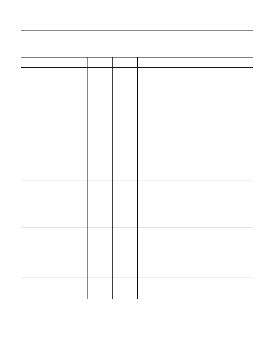
SPECIFICATIONS
(V
DD
= +2.7 V to +5.5 V; R
L
= 2 k to GND; C
L
= 200 pF to GND; V
REF
= V
DD
; all specifications T
MIN
to T
MAX
unless otherwise noted)
Table 1.
Parameter A
Grade
3
B
Grade
3
Unit
Conditions/Comments
STATIC PERFORMANCE
1
Resolution
16
16
Bits min
Relative Accuracy
±32
tbd
LSB max
Differential Nonlinearity
±1
±1
LSB max
Guaranteed Monotonic by Design.
Load Regulation
2
2
LSB/mA
VDD=Vref=5V, Midscale Iout=0mA to 15mA
sourcing/sinking
LSB/mA
VDD=Vref=3V, Midscale Iout=0mA to 7.5mA
sourcing/sinking
Zero Code Error
+2
+2
mV typ
All Zeroes Loaded to DAC Register
+10
+10
mV
max
Offset Error
±10
±10
mV max
Full-Scale Error
-0.15
-0.15
% of FSR typ
All Ones Loaded to DAC Register.
-1
-1
% of FSR max
Gain Error
±1. 5
±1. 5
% of FSR max
Zero Code Error Drift
2
±2
±2
µV/°C
typ
Gain Temperature Coefficient
±2.5
±2.5
ppm typ
of FSR/°C
Offset Temperature Coefficient 1.7
1.7
µV/°C typ
DC Power Supply Rejection Ratio
-100
-100
dB typ
DAC code = midscale; V
DD
= 5V ±10%
DC Crosstalk
6
10 10
µV typ
R
L
= 2 k. to GND or V
DD
4.5 4.5
µV/mA typ
Due to Load current change
-10 -10
µV typ
Due to Powering Down (per channel)
OUTPUT CHARACTERISTICS
1
Output Voltage Range
0 0
V min
V
DD
V
DD
V max
Capacitive Load Stability
2
2
nF typ
R
L
=
10
10
nF
typ
R
L
=2 k
DC Output Impedance
0.5
0.5
typ
Short Circuit Current
30
30
mA typ
V
DD
=+5V
Power-Up Time
4
4
µs typ
Coming Out of Power-Down Mode. V
DD
=+5V
REFERENCE INPUT
Reference Input voltage
V
DD
V
DD
V
±1% for specified performance
Reference Current
40
40
µA typ
V
REF
= V
DD
= 5 V
75
75
µA max
Reference Current
30
30
µA typ
V
REF
= V
DD
= 3.6 V
50
50
µA max
Reference Input Range
0.75
0.75
V min
V
DD
V
DD
V max
Reference Input Impedance
150
150
k
typ
Per DAC channel
LOGIC INPUTS
2
Input Current
±2
±2
µA max
All digital inputs
V
INL
, Input Low Voltage
0.8
0.8
V max
V
DD
=+5 V, +3 V
V
INH
, Input High Voltage
2
2
V min
V
DD
=+5 V, +3 V
1
Linearity calculated using a reduced code range: AD5664 ( Code 512 to code 65024);. Output unloaded.
2
Guaranteed by design and characterization, not production tested.
3
. Temperature Range: A grade (-40°C to +105°C); B grade (-40°C to +105°C)
AD5664
Preliminary Technical Data
Rev. PrA
| Page 4 of 28
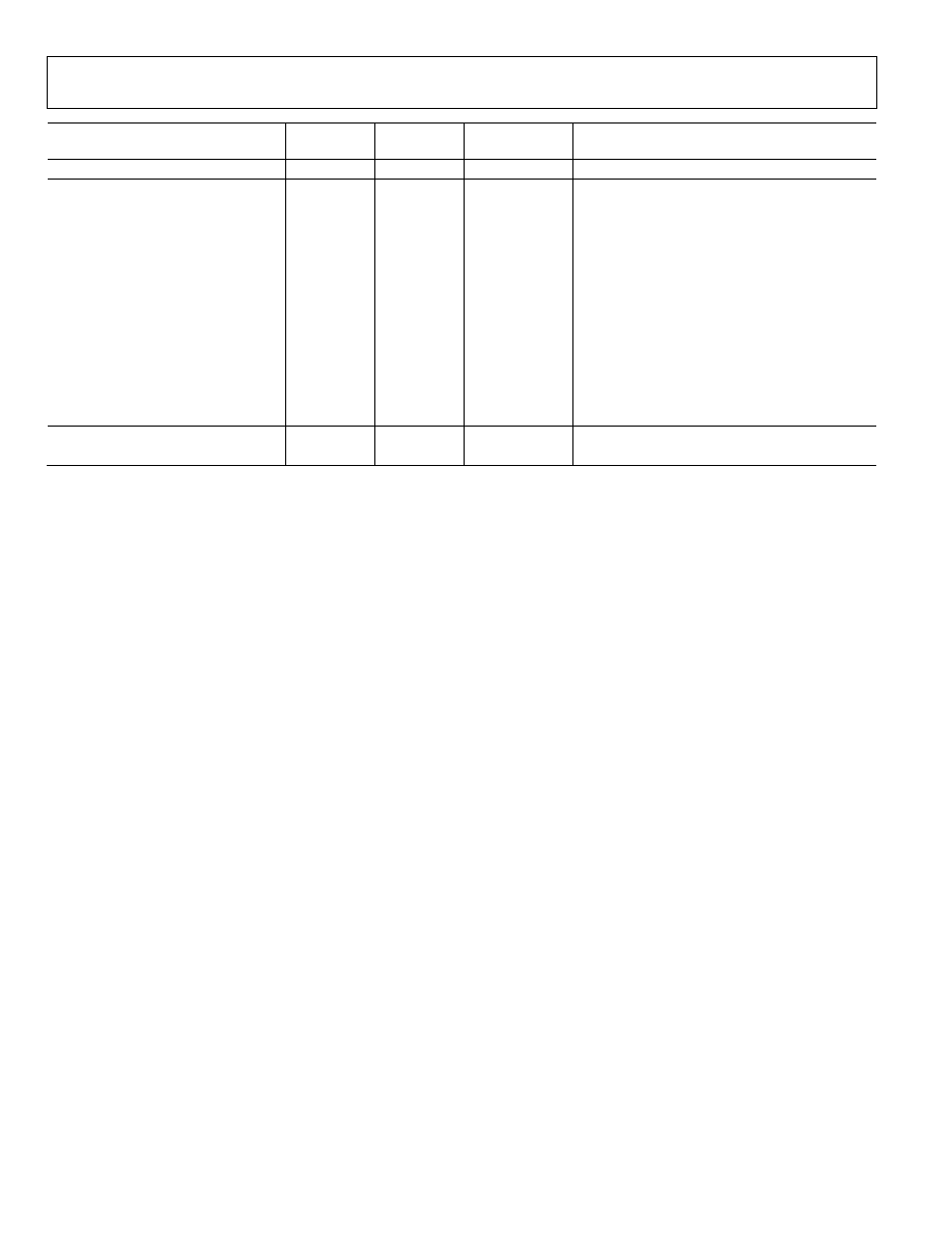
Parameter A
Grade
3
B
Grade
3
Unit
Conditions/Comments
Pin Capacitance
3
3
pF typ
POWER REQUIREMENTS
V
DD
2.7
2.7
V min
All Digital Inputs at 0 or V
DD
5.5
5.5
V max
DAC Active and Excluding Load Current
I
DD
(Normal Mode)
V
DD
=4.5 V to +5.5 V
0.6
0.6
mA typ
V
IH
=V
DD
and V
IL
=GND
V
DD
=4.5 V to +5.5 V
0.9
0.9
mA max
V
IH
=V
DD
and V
IL
=GND
V
DD
=2.7V to +3.6 V
0.5
0.5
mA typ
V
IH
=V
DD
and V
IL
=GND
V
DD
=2.7V to +3.6 V
0.7
0.7
mA max
V
IH
=V
DD
and V
IL
=GND
I
DD
(All Power-Down Modes)
V
DD
=4.5 V to +5.5 V
0.48
0.48
µA typ
V
IH
=V
DD
and V
IL
=GND
V
DD
=4.5 V to +5.5 V
1
1
µA max
V
IH
=V
DD
and V
IL
=GND
V
DD
=2.7V to +3.6V
0.1
0.1
µA typ
V
IH
=V
DD
and V
IL
=GND
V
DD
=2.7V to +3.6V
1
1
µA max
V
IH
=V
DD
and V
IL
=GND
POWER EFFICIENCY
I
OUT
/I
DD
90
90
%
I
LOAD
=2 mA, V
DD
=+5 V
4
Output unloaded.
5
Reference input range at ambient where ±1 LSB max DNL specification is achievable.
Preliminary Technical Data
AD5664
Rev. PrA | Page 5 of 28
AC CHARACTERISTICS
1
(V
DD
= +2.7 V to +5.5 V; R
L
= 2 k to GND; C
L
= 200 pF to GND; Vref = V
DD
; all specifications T
MIN
to T
MAX
unless otherwise noted)
Parameter
2
Min
Typ
Max
Unit
Conditions/Comments
Output Voltage Settling Time
8
10
µs
¼ to ¾ scale settling to ±2LSB
Settling Time for 1LSB Step
Slew Rate
1.5
V/µs
Digital-to-Analog Glitch Impulse
10
nV-s
1 LSB Change Around Major Carry.
Channel to-Channel Isolation
100
dB
Digital Feedthrough
0.5
nV-s
Digital Crosstalk
0.5
nV-s
Analog Crosstalk
1
nV-s
DAC-to-DAC Crosstalk
3
nV-s
Multiplying Bandwidth
200
kHz
VREF = 2V ± 0.1 V p-p.
Total Harmonic Distortion
-80
dB
VREF = 2V ± 0.1 V p-p. Frequency = 10kHz
Output Noise Spectral Density
120
nV/Hz
DAC code=8400
H
, 1kHz
100
nV/Hz
DAC code=8400
H
, 10kHz
Output Noise
15
µVp-p
0.1Hz to 10Hz;
NOTES
1
Guaranteed by design and characterization; not production tested.
2
See the Terminology section.
3
Temperature range (B Version): 40
°C to +105°C; typical at +25°C.
AD5664
Preliminary Technical Data
Rev. PrA
| Page 6 of 28
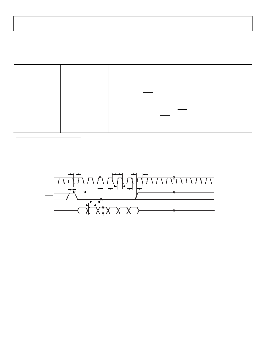
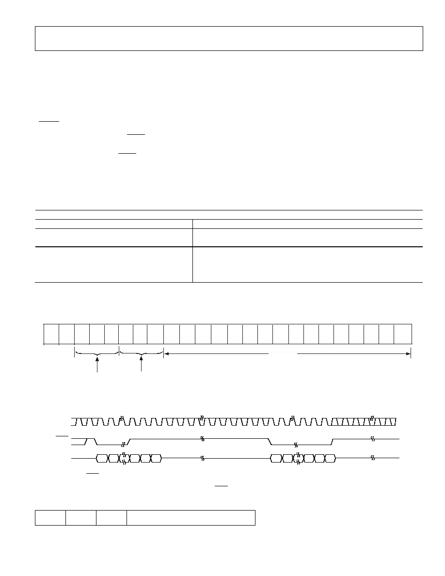
TIMING CHARACTERISTICS
All input signals are specified with tr = tf = 1 ns/V (10% to 90% of V
DD
) and timed from a voltage level of (V
IL
+ V
IH
)/2. See Figure 2.
V
DD
= 2.7 V to 5.5 V; all specifications T
MIN
to T
MAX
, unless otherwise noted.
Table 2.
Limit at T
MIN
, T
MAX
Parameter V
DD
= 2.7 V to 5.5 V
Unit
Conditions/Comments
t
1
2
20
ns min
SCLK cycle time
t
2
9
ns min
SCLK high time
t
3
9
ns min
SCLK low time
t
4
13 ns
min
SYNC to SCLK falling edge setup time
t
5
4
ns min
Data setup time
t
6
4
ns min
Data hold time
t
7
0 ns
min
SCLK falling edge to SYNC rising edge
T
8
50 ns
min
Minimum SYNC high time
t
9
13 ns
min
SYNC rising edge to sclk fall ignore
t
10
0 ns
min
SCLK falling edge to SYNC fall ignore
2
Maximum SCLK frequency is 50 MHz at V
DD
= 3.6 V to 5.5 V, and tbd MHz at V
DD
= 2.7 V to 3.6 V.
DIN
SYNC
SCLK
DB23
DB0
t
9
t
10
t
4
t
3
t
2
t
7
t
6
t
5
t
1
t
8
04777-002
Figure 2. Serial Write Operation
Preliminary Technical Data
AD5664
Rev. PrA | Page 7 of 28
ABSOLUTE MAXIMUM RATINGS
T
A
= 25°C, unless otherwise noted.
Table 3.
Parameter Rating
V
DD
to GND
-0.3 V to +7 V
V
OUT
to GND
-0.3 V to V
DD
+ 0.3 V
V
REF
to GND
-0.3 V to V
DD
+ 0.3 V
Digital Input Voltage to GND
-0.3 V to V
DD
+ 0.3 V
Operating Temperature Range
Industrial (A, B Version)
-40°C to +105°C
Storage Temperature Range
-65°C to +150°C
Junction Temperature (T
J
max) 150°C
Power Dissipation
(T
J
max - T
A
)/
JA
LFCSP Package (4-Layer Board)
JA
Thermal Impedance
61°C/W
MSOP Package (4-Layer Board)
JA
Thermal Impedance
142°C/W
JC
Thermal Impedance
43.7°C/W
Reflow Soldering Peak Temperature
Pb-free
260°C± 5°C
ESD 2
kV
Stresses above those listed under Absolute Maximum Ratings
may cause permanent damage to the device. This is a stress
rating only; functional operation of the device at these or any
other conditions above those listed in the operational sections
of this specification is not implied. Exposure to absolute
maximum rating conditions for extended periods may affect
device reliability.
ESD CAUTION
ESD (electrostatic discharge) sensitive device. Electrostatic charges as high as 4000 V readily accumulate on
the human body and test equipment and can discharge without detection. Although this product features
proprietary ESD protection circuitry, permanent damage may occur on devices subjected to high energy
electrostatic discharges. Therefore, proper ESD precautions are recommended to avoid performance
degradation or loss of functionality.
AD5664
Preliminary Technical Data
Rev. PrA
| Page 8 of 28
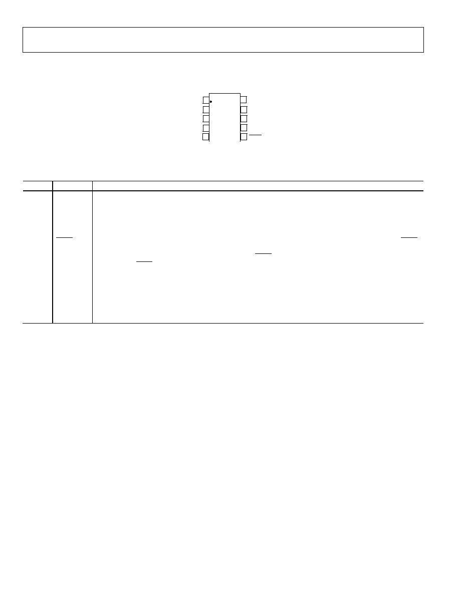
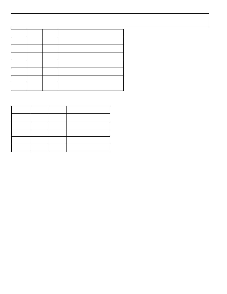
PIN CONFIGURATION AND FUNCTION DESCRIPTION
TOP VIEW
(Not to Scale)
8
7
6
1
2
3
4
AD5664
5
10
9
SYNC
VOUTA
DIN
GND
V
DD
SCLK
VOUTB
VOUTD
VOUTC
VREF
Figure 3. MSOP and LFCSP Pin Configuration
Table 4. Pin Function Descriptions
Pin No. Mnemonic Function
1 V
OUT
A
Analog Output Voltage from DAC A. The output amplifier has rail-to-rail operation.
2 V
OUT
B
Analog Output Voltage from DAC B. The output amplifier has rail-to-rail operation.
3
GND
Ground Reference Point for All Circuitry on the Part.
4 V
OUT
C
Analog Output Voltage from DAC C. The output amplifier has rail-to-rail operation.
5 V
OUT
D
Analog Output Voltage from DAC D. The output amplifier has rail-to-rail operation.
6
SYNC
Level-Triggered Control Input (Active Low). This is the frame synchronization signal for the input data. When SYNC
goes low, it enables the input shift register, and data is transferred in on the falling edges of the following clocks.
The DAC is updated following the 24
th
clock cycle unless SYNC is taken high before this edge, in which case the
rising edge of SYNC acts as an interrupt and the write sequence is ignored by the DAC.
7 SCLK
Serial Clock Input. Data is clocked into the input shift register on the falling edge of the serial clock input. Data can
be transferred at rates up to 50 MHz.
8 DIN
Serial Data Input. This device has a 24-bit shift register. Data is clocked into the register on the falling edge of the
serial clock input.
9 V
DD
Power Supply Input. These parts can be operated from 2.7 V to 5.5 V. V
DD
should be decoupled to GND.
10 V
REF
Reference Voltage Input.

Preliminary Technical Data
AD5664
Rev. PrA | Page 9 of 28
TYPICAL PERFORMANCE CHARACTERISTICS
TBD
Figure 4. Typical INL Plot
TBD
Figure 5. Typical DNL Plot
TBD
Figure 6. Typical Total Unadjusted Error Plot
TBD
Figure 7. INL Error and DNL Error vs. Temperature
TBD
Figure 8. INL and DNL Error vs. V
REF
TBD
Figure 9. INL and DNL Error vs. Supply
TBD
Figure 10. Gain Error and Full-Scale Error vs. Temperature

AD5664
Preliminary Technical Data
Rev. PrA
| Page 10 of 28
TBD
Figure 11. Zero-Scale and Offset Error vs. Temperature
TBD
Figure 12. Gain Error and Full-Scale Error vs. Supply
TBD
Figure 13. Zero-Scale and Offset Error vs. Supply
TBD
Figure 14. I
DD
Histogram with V
DD
= 5.5 V
TBD
Figure 15. Headroom at Rails vs. Source and Sink Current
TBD
Figure 16. Supply Current vs. Code
TBD
Figure 17. Supply Current vs. Temperature

Preliminary Technical Data
AD5664
Rev. PrA | Page 11 of 28
TBD
Figure 18. Supply Current vs. Supply Voltage
TBD
Figure 19. Supply Current vs. Logic Input Voltage
TBD
Figure 20. Full-Scale Settling Time, 3 V
TBD
Figure 21. Full-Scale Settling Time, 5 V
TBD
Figure 22. Power-On Reset to 0 V
TBD
Figure 23. Power-On Reset to Midscale

AD5664
Preliminary Technical Data
Rev. PrA
| Page 12 of 28
TBD
Figure 24. Exiting Power-Down to Midscale
TBD
Figure 25. Digital-to-Analog Glitch Impulse (Negative)
TBD
Figure 26. Digital-to-Analog Glitch Impulse (Positive)
TBD
Figure 27. Digital Feedthrough
TBD
Figure 28. Total Harmonic Distortion
TBD
Figure 29. Settling Time vs. Capacitive Load
TBD
Figure 30. 0.1 Hz to 10 Hz Output Noise Plot

Preliminary Technical Data
AD5664
Rev. PrA | Page 13 of 28
TBD
Figure 31. Noise Spectral Density

AD5664
Preliminary Technical Data
Rev. PrA
| Page 14 of 28
TERMINOLOGY
Relative Accuracy or Integral Nonlinearity (INL)
For the DAC, relative accuracy or integral nonlinearity is a
measurement of the maximum deviation, in LSBs, from a
straight line passing through the endpoints of the DAC transfer
function. A typical INL vs. code plot can be seen in Figure 4.
Differential Nonlinearity (DNL)
Differential nonlinearity is the difference between the measured
change and the ideal 1 LSB change between any two adjacent
codes. A specified differential nonlinearity of ±1 LSB maximum
ensures monotonicity. This DAC is guaranteed monotonic by
design. A typical DNL vs. code plot can be seen in Figure 5.
Zero-Code Error
Zero-code error is a measurement of the output error when
zero code (0x0000) is loaded to the DAC register. Ideally, the
output should be 0 V. The zero-code error is always positive in
the AD5664 because the output of the DAC cannot go below
0 V. It is due to a combination of the offset errors in the DAC
and the output amplifier. Zero-code error is expressed in mV. A
plot of zero-code error vs. temperature can be seen in Figure 11.
Full-Scale Error
Full-scale error is a measurement of the output error when full-
scale code (0xFFFF) is loaded to the DAC register. Ideally, the
output should be V
DD
- 1 LSB. Full-scale error is expressed in
percent of full-scale range. A plot of full-scale error vs.
temperature can be seen in Figure 10.
Gain Error
This is a measure of the span error of the DAC. It is the deviation
in slope of the DAC transfer characteristic from ideal expressed
as a percent of the full-scale range.
Total Unadjusted Error (TUE)
Total unadjusted error is a measurement of the output error,
taking all the various errors into account. A typical TUE vs.
code plot can be seen in Figure 6.
Zero-Code Error Drift
This is a measurement of the change in zero-code error with a
change in temperature. It is expressed in µV/°C.
Gain Temperature Coefficient
This is a measurement of the change in gain error with changes
in temperature. It is expressed in (ppm of full-scale range)/°C.
Offset Error
Offset error is a measure of the difference between V
OUT
(actual) and V
OUT
(ideal) expressed in mV in the linear region of
the transfer function. Offset error is measured on the AD5664
with code 512 loaded in the DAC register.
It can be negative or
positive.
DC Power Supply Rejection Ratio (PSRR)
This indicates how the output of the DAC is affected by changes in
the supply voltage. PSRR is the ratio of the change in V
OUT
to a
change in V
DD
for full-scale output of the DAC. It is measured in
dB. V
REF
is held at 2 V, and V
DD
is varied by ±10%.
Output Voltage Settling Time
This is the amount of time it takes for the output of a DAC to settle
to a specified level for a ¼ to ¾ full-scale input change and is
measured from the 24
th
falling edge of SCLK.
Digital-to-Analog Glitch Impulse
Digital-to-analog glitch impulse is the impulse injected into the
analog output when the input code in the DAC register changes
state. It is normally specified as the area of the glitch in nV-s,
and is measured when the digital input code is changed by
1 LSB at the major carry transition (0x7FFF to 0x10000). See
Figure 25 and Figure 26.
Digital Feedthrough
Digital feedthrough is a measure of the impulse injected into
the analog output of the DAC from the digital inputs of the
DAC, but is measured when the DAC output is not updated. It
is specified in nV-s, and measured with a full-scale code change
on the data bus, that is, from all 0s to all 1s and vice versa.
Total Harmonic Distortion (THD)
This is the difference between an ideal sine wave and its attenuated
version using the DAC. The sine wave is used as the reference for
the DAC, and the THD is a measurement of the harmonics present
on the DAC output. It is measured in dB.
Noise Spectral Density
This is a measurement of the internally generated random noise.
Random noise is characterized as a spectral density (voltage per
Hz). It is measured by loading the DAC to m
idscale and meas-
uring noise at the output. It is measured in nV/Hz. A plot of
Noise Spectral Density can be seen in Figure 31.
DC Crosstalk
This is the dc change in the output level of one DAC in response to
a change in the output of another DAC. It is measured with a full-
scale output change on one DAC while monitoring another DAC
kept at midscale. It is expressed in µV.
Channel-to-Channel Isolation
This is the ratio of the amplitude of the signal at the output of one
DAC to a sine wave on the reference input of another DAC. It is
measured in dB.
Digital Crosstalk
This is the glitch impulse transferred to the output of one DAC at
midscale in response to a full-scale code change (all 0s to all 1s and

Preliminary Technical Data
AD5664
Rev. PrA | Page 15 of 28
vice versa) in the input register of another DAC. It is measured in
standalone mode and is expressed in nV-s.
Analog Crosstalk
This is the glitch impulse transferred to the output of one DAC due
to a change in the output of another DAC. It is measured by
loading one of the input registers with a full-scale code change (all
0s to all 1s and vice versa) while keeping LDAC high. Then pulse
LDAC low and monitor the output of the DAC whose digital code
was not changed. The area of the glitch is expressed in nV-s.
DAC-to-DAC Crosstalk
This is the glitch impulse transferred to the output of one DAC due
to a digital code change and subsequent output change of another
DAC. This includes both digital and analog crosstalk. It is
measured by loading one of the DACs with a full-scale code change
(all 0s to all 1s and vice versa) with LDAC low and monitoring the
output of another DAC. The energy of the glitch is expressed in
nV-s.
Multiplying Bandwidth
The amplifiers within the DAC have a finite bandwidth. The
multiplying bandwidth is a measure of this. A sine wave on the
reference (with full-scale code loaded to the DAC) appears on the
output. The multiplying bandwidth is the frequency at which the
output amplitude falls to 3 dB below the input.
AD5664
Preliminary Technical Data
Rev. PrA
| Page 16 of 28
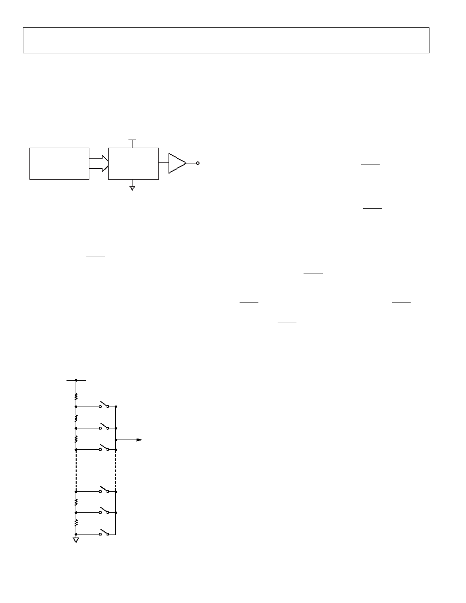
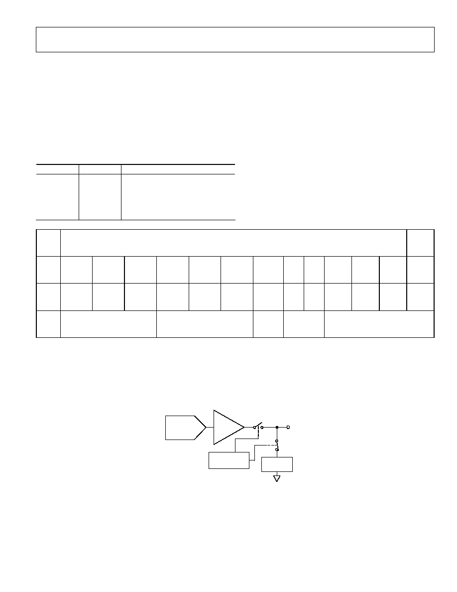
THEORY OF OPERATION
D/A SECTION
The AD5664 DAC is fabricated on a CMOS process. The
architecture consists of a string DAC followed by an output
buffer amplifier. Figure 32 shows a block diagram of the DAC
architecture.
V
OUT
OUTPUT
AMPLIFIER
(Gain=2)
V
DD
GND
RESISTOR
STRING
REF (+)
REF ()
DAC REGISTER
Figure 32. DAC Architecture
Since the input coding to the DAC is straight binary, the ideal
output voltage is given by
×
=
65,536
D
V
V
REF
OUT
where D is the decimal equivalent of the binary code that is
loaded to the DAC register. It can range from 0 to 65535.
RESISTOR STRING
The resistor string section is shown in Figure 33. It is simply a
string of resistors, each of value R. The code loaded to the DAC
register determines at which node on the string the voltage is
tapped off to be fed into the output amplifier. The voltage is
tapped off by closing one of the switches connecting the string
to the amplifier. Because it is a string of resistors, it is guaranteed
monotonic.
R
R
R
R
R
TO OUTPUT
AMPLIFIER
04777-023
Figure 33. Resistor String
OUTPUT AMPLIFIER
The output buffer amplifier can generate rail-to-rail voltages on
its output, which gives an output range of 0 V to V
DD
. It can drive
a load of 2 k in parallel with 1000 pF to GND. The source and
sink capabilities of the output amplifier can be seen in Figure 15.
The slew rate is 1.5 V/µs with a ¼ to ¾ full-scale settling time of
10 µs.
SERIAL INTERFACE
The AD5664 has a 3-wire serial interface (SYNC, SCLK, and
DIN) that is compatible with SPI, QSPI, and MICROWIRE
interface standards as well as with most DSPs. See Figure 2 for
a timing diagram of a typical write sequence.
The write sequence begins by bringing the SYNC line low. Data
from the DIN line is clocked into the 24-bit shift register on the
falling edge of SCLK. The serial clock frequency can be as high
as 50 MHz, making the AD5664 compatible with high speed
DSPs. On the 24
th
falling clock edge, the last data bit is clocked
in and the programmed function is executed, that is, a change
in DAC register contents and/or a change in the mode of opera-
tion. At this stage, the SYNC line can be kept low or be brought
high. In either case, it must be brought high for a minimum of
33 ns before the next write sequence so that a falling edge of
SYNC can initiate the next write sequence. Since the SYNC
buffer draws more current when V
IN
= 2.0 V than it does when
V
IN
= 0.10 V, SYNC should be idled low between write
sequences for even lower power operation. As mentioned
previously it must, however, be brought high again just before
the next write sequence.
Preliminary Technical Data
AD5664
Rev. PrA | Page 17 of 28
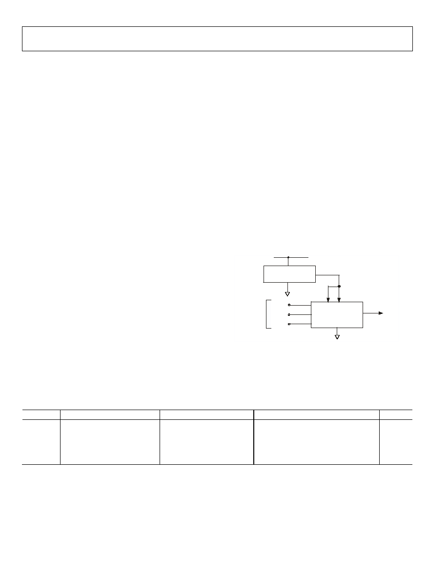
INPUT SHIFT REGISTER
The input shift register is 24 bits wide (see Figure 34). The first
two bits are don't cares. The next three are the Command bits
C2 C0, (see Table 1) ) followed by the 3-bit DAC address A2-
A0, (see Table 2) and finally the 16-bit data word. These are
transferred to the DAC register on the 24
th
falling edge of SCLK.
SYNC INTERRUPT
In a normal write sequence, the SYNC line is kept low for at
least 24 falling edges of SCLK, and the DAC is updated on the
24
th
falling edge. However, if SYNC is brought high before the
24
th
falling edge, this acts as an interrupt to the write sequence.
The shift register is reset and the write sequence is seen as
invalid. Neither an update of the DAC register contents nor a
change in the operating mode occurs (see Figure 35).
POWER-ON RESET
The AD5664 family contains a power-on reset circuit that
controls the output voltage during power-up. The AD5664 DAC
outputs power up to 0 V and the output remains there until a
valid write sequence is made to the DAC. This is useful in
applications where it is important to know the state of the
output of the DAC while it is in the process of powering up.
Software Reset
The AD5664 contains a Software Reset function. Command
110 is reserved for the Software Reset function, see Table 1. The
Software Reset command contains two reset modes that are
software-programmable by setting bit DB0 in the control
register. Table 5 shows how the state of the bit corresponds to
the mode of operation of the device.
Table 5. Software Reset Modes for the AD5664
Software Reset Mode
DB0
Registers reset to zero
0 DAC
Register
Input
Register
1 (Power-on -Reset)
DAC Register
Input
Register
/LDAC
Register
Powerdown
Register
DATA BITS
DB0 (LSB)
DB23 (MSB)
X
X
C2
C1
C0
A2
A1
A0
D15
D14
D13
D12
D11
D10
D9
D8
D7
D6
D5
D4
D3
D2
D1
D0
ADDRESS BITS
COMMAND BITS
Figure 34. Input Register Contents
04777-025
DIN
DB23
DB23
DB0
DB0
INVALID WRITE SEQUENCE:
SYNC HIGH BEFORE 24
TH
FALLING EDGE
VALID WRITE SEQUENCE, OUTPUT UPDATES
ON THE 24
TH
FALLING EDGE
SYNC
SCLK
Figure 35. SYNC Interrupt Facility
C2 C1 C0 Command
AD5664
Preliminary Technical Data
Rev. PrA
| Page 18 of 28
0
0
0
Write to Input Register n
0
0
1
Update DAC Register n
0
1
0
Write to Input Register n, Update All
0
1
1
Write to and Update DAC channel n
1
0
0
Power Down DAC (Power-up)
1 0 1 Reset
(Power-on-Reset)
1 1 0 Load
LDAC
Register
1 1 1 Reserved
Table 1. Command Definition
A2 A1 A0 ADDRESS
(n)
0 0 0 DAC
A
0 0 1 DAC
B
0 1 0 DAC
C
0 1 1 DAC
D
1 1 1 All
DACs
Table 2. Address Command
Preliminary Technical Data
AD5664
Rev. PrA | Page 19 of 28
POWER-DOWN MODES
The AD5664 contains four separate modes of operation. Command 100 is reserved for the Power-Down function. See Table 1. These
modes are software-programmable by setting two bits (DB5 and DB4) in the control register. Table 6 shows how the state of the bits
corresponds to the mode of operation of the device. Any or all DACs, (DacD to DacA) may be powered down to the selected mode by
setting the corresponding 4 bits (DB3,2,1,0) to a "1". By executing the same Command 100, any combination of DACs may be powered
up by setting the bits (DB5 and DB4) to Normal Operation mode. Again, to select which combination of DAC channels to power-up set
the corresponding 4 bits (DB3, 2, 1, 0) to a "1". See Table 7 for contents of the Input Shift Register during power down/up operation.
The DAC output will power-up to the value in the input register while /LDAC is low. If /LDAC is high, the DAC ouput will power-up to
the value held in the DAC register before power-down.
Table 6. Modes of Operation for the AD5664
DB5
DB4
Operating Mode
0
0
Normal Operation
Power-Down
Modes
0
1
1 k to GND
1
0
100 k to GND
1 1
Three-State
MSB
LSB
DB23
DB22
DB21 DB20 DB19 DB18 DB17 DB16 DB15--
DB6
DB5 DB4 DB3
DB2 DB1 DB0
x
1 0 0 x x x x PD1
PD0
DacD
DacC
DacB
DacA
Don't
Cares
COMMAND BITS (C2-C0)
ADDRESS BITS (A2 A0)
Don't cares
Don't
Cares
Power Down
Mode
Power Down/Up Channel Selection Set
Bit to a "1" to select channel
Table 7. 24-Bit Input Shift Register Contents of Power Up/Down Function
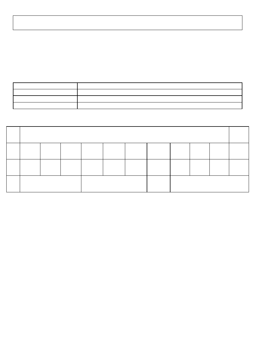
When both bits are set to 0, the part works normally with its normal power consumption of 500 µA at 5 V. However, for the three power-
down modes, the supply current falls to 480 nA at 5 V (100 nA at 3 V). Not only does the supply current fall, but the output stage is also
internally switched from the output of the amplifier to a resistor network of known values. This has the advantage that the output
impedance of the part is known while the part is in power-down mode. The outputs can either be connected internally to GND through a
1 k or 100 k resistor, or left open-circuited (three-state) (see Figure 36).
RESISTOR
NETWORK
V
OUT
RESISTOR
STRING DAC
04777-026
POWER-DOWN
CIRCUITRY
AMPLIFIER
Figure 36. Output Stage During Power-Down
The bias generator, the output amplifier, the resistor string, and other associated linear circuitry are shut down when power-down mode is
activated. However, the contents of the DAC register are unaffected when in power-down. The time to exit power-down is typically 4 µs
for V
DD
= 5 V and for V
DD
= 3 V (see Figure 24).
AD5664
Preliminary Technical Data
Rev. PrA
| Page 20 of 28
LDAC FUNCTION
The AD5664 does not have a hardware /LDAC pin. Writing to the DAC using command 110, allows one to perform a software /LDAC
on any or all of the DAC channels. The DAC channels are selected by setting the bits of the 4-bit /LDAC register (DB3,DB2, DB1,DB0).
See Table 8 for the software /LDAC mode of operation. Setting the /LDAC bit to a "1" means the DAC registers are automatically
updated after new data is read in on the falling edge of the 24
th
SCLK pulse. This is equivalent to having an /LDAC hardware pin tied
permanently low for the selected DAC channel. See Table 9 for contents of the Input Shift Register during the /LDAC overwrite mode of
operation.
Load DAC Register
/LDACBITS (DB3-DB0)
/LDAC Operation
0
Normal operation - default
1
The DAC registers are updated after new data is read in on the falling edge of the 24th SCLK pulse.
Table 8. Software LDAC Definition
MSB
LSB
DB23
DB22
DB21 DB20 DB19 DB18 DB17 DB16
DB15 - DB4
DB3 DB2 DB1 DB0
x
1 0 1 x x x x DacD
DacC
DacB
DacA
Don't
Cares
COMMAND BITS (C2-C0)
ADDRESS BITS (A3 A0)
Don't cares
Don't Cares
Setting bit to "1" selects DAC channel for /LDAC
operation mode.
Table 9. 24-Bit Input Shift Register Contents for /LDAC Overwrite Function
Preliminary Technical Data
AD5664
Rev. PrA | Page 21 of 28
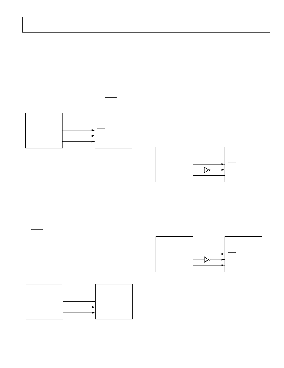
MICROPROCESSOR INTERFACING
AD5664 to Blackfin® ADSP-BF53X Interface
Figure 37 shows a serial interface between the AD5664 and the
Blackfin ADSP-BF53X microprocessor. The ADSP-BF53X processor
family incorporates two dual-channel synchronous serial ports,
SPORT1 and SPORT0, for serial and multiprocessor communica-
tions. Using SPORT0 to connect to the AD5664, the setup for the
interface is as follows. DT0PRI drives the DIN pin of the AD5664,
while TSCLK0 drives the SCLK of the part. The
SYNC
is driven
from TFS0.
AD5662*
*ADDITIONAL PINS OMITTED FOR CLARITY
TFS0
DTOPRI
TSCLK0
SYNC
DIN
SCLK
04777-027
ADSP-BF53X*
Figure 37. AD5664 to Blackfin ADSP-BF53X Interface
AD5664 to 68HC11/68L11 Interface
Figure 38 shows a serial interface between the AD5664 and the
68HC11/68L11 microcontroller. SCK of the 68HC11/68L11
drives the SCLK of the AD5664, while the MOSI output drives
the serial data line of the DAC.
The SYNC signal is derived from a port line (PC7). The setup
conditions for correct operation of this interface are as follows.
The 68HC11/68L11 is configured with its CPOL bit as a 0 and
its CPHA bit as a 1. When data is being transmitted to the DAC,
the SYNC line is taken low (PC7). When the 68HC11/68L11 is
configured as described above, data appearing on the MOSI
output is valid on the falling edge of SCK. Serial data from the
68HC11/68L11 is transmitted in 10-bit bytes with only eight
falling clock edges occurring in the transmit cycle. Data is
transmitted MSB first. In order to load data to the AD5664, PC7
is left low after the first eight bits are transferred, and a second
serial write operation is performed to the DAC; PC7 is taken
high at the end of this procedure.
AD5662*
*ADDITIONAL PINS OMITTED FOR CLARITY
PC7
SCK
MOSI
SYNC
SCLK
DIN
04777-028
68HC11/68L11*
Figure 38. AD5664 to 68HC11/68L11 Interface
AD5664 to 80C51/80L51 Interface
Figure 39 shows a serial interface between the AD5664 and the
80C51/80L51 microcontroller. The setup for the interface is as
follows. TXD of the 80C51/80L51 drives SCLK of the AD5664,
while RXD drives the serial data line of the part. The SYNC
signal is again derived from a bit-programmable pin on the port.
In this case, port line P3.3 is used. When data is to be transmitted
to the AD5664, P3.3 is taken low. The 80C51/80L51 transmits
data in 10-bit bytes only; thus only eight falling clock edges
occur in the transmit cycle. To load data to the DAC, P3.3 is left
low after the first eight bits are transmitted, and a second write
cycle is initiated to transmit the second byte of data. P3.3 is
taken high following the completion of this cycle. The
80C51/80L51 outputs the serial data in a format that has the
LSB first. The AD5664 must receive data with the MSB first.
The 80C51/80L51 transmit routine should take this into account.
80C51/80L51*
AD5662*
*ADDITIONAL PINS OMITTED FOR CLARITY
P3.3
TXD
RXD
SYNC
SCLK
DIN
04777-029
Figure 39. AD5664 to 80C51/80L51 Interface
AD5664 to MICROWIRE Interface
Figure 40 shows an interface between the AD5664 and any
MICROWIRE-compatible device. Serial data is shifted out on
the falling edge of the serial clock and is clocked into the AD5664
on the rising edge of the SK.
MICROWIRE*
AD5662*
*ADDITIONAL PINS OMITTED FOR CLARITY
CS
SK
SO
SYNC
SCLK
DIN
04777-030
Figure 40. AD5664 to MICROWIRE Interface
AD5664
Preliminary Technical Data
Rev. PrA
| Page 22 of 28
APPLICATIONS
CHOOSING A REFERENCE FOR THE AD5664
To achieve the optimum performance from the AD5664,
thought should be given to the choice of a precision voltage
reference. The AD5664 has only one reference input, V
REF
. The
voltage on the reference input is used to supply the positive
input to the DAC. Therefore any error in the reference is
reflected in the DAC.
When choosing a voltage reference for high accuracy applica-
tions, the sources of error are initial accuracy, ppm drift, long
term drift, and output voltage noise. Initial accuracy on the
output voltage of the DAC leads to a full-scale error in the
DAC. To minimize these errors, a reference with high initial
accuracy is preferred. Also, choosing a reference with an output
trim adjustment, such as the ADR423, allows a system designer
to trim system errors out by setting a reference voltage to a
voltage other than the nominal. The trim adjustment can also
be used at temperature to trim out any error.
Long-term drift is a measurement of how much the reference
drifts over time. A reference with a tight long-term drift
specification ensures that the overall solution remains relatively
stable during its entire lifetime.
The temperature coefficient of a reference's output voltage
affect INL, DNL, and TUE. A reference with a tight temperature
coefficient specification should be chosen to reduce temperature
dependence of the DAC output voltage in ambient conditions.
In high accuracy applications, which have a relatively low noise
budget, reference output voltage noise needs to be considered. It
is important to choose a reference with as low an output noise
voltage as practical for the system noise resolution required.
Precision voltage references such as the ADR425 produce low
output noise in the 0.1 Hz to10 Hz range. Examples of recom-
mended precision references for use as supply to the AD5664
are shown in the Table 7.
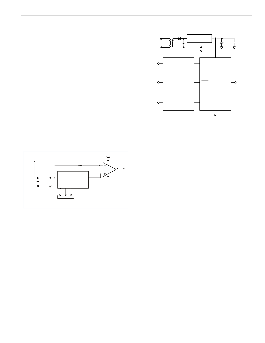
USING A REFERENCE AS A POWER SUPPLY FOR
THE AD5664
Because the supply current required by the AD5664 is extremely
low, an alternative option is to use a voltage reference to supply
the required voltage to the part (see Figure 41). This is especially
useful if the power supply is quite noisy, or if the system supply
voltages are at some value other than 5 V or 3 V, for example,
15 V. The voltage reference outputs a steady supply voltage for
the AD5664; see Table 7 for a suitable reference. If the low drop-
out REF195 is used, it must supply 500 µA of current to the
AD5664, with no load on the output of the DAC. When the
DAC output is loaded, the REF195 also needs to supply the
current to the load. The total current required (with a 5 k
load on the DAC output) is
500 µA + (5 V/5 k) = 1.5 mA
The load regulation of the REF195 is typically 2 ppm/mA,
which results in a 3 ppm (15 µV) error for the 1.5 mA current
drawn from it. This corresponds to a 0.196 LSB error.
THREE-WIRE
SERIAL
INTERFACE
SYNC
SCLK
DIN
+15V
+5V
500 A
V
OUT
= 0V TO 5V
AD5664
REF195
V
DD
V
REF
Figure 41. REF195 as Power Supply to the AD5664
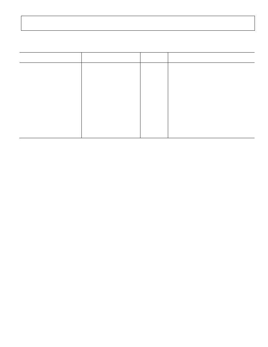
Table 7. Partial List of Precision References for Use with the AD5664
Part No.
Initial Accuracy (mV max)
Temp Drift (ppm
o
C max)
0.1 Hz to 10 Hz Noise (µV p-p typ)
V
OUT
(V)
ADR425 ±2
3
3.4
5
ADR395 ±6
25
5
5
REF195 ±2
5
50
5
AD780 ±2
3
4
2.5/3
ADR423 ±2
3
3.4
3
Preliminary Technical Data
AD5664
Rev. PrA | Page 23 of 28
BIPOLAR OPERATION USING THE AD5664
The AD5664 has been designed for single-supply operation,
but a bipolar output range is also possible using the circuit in
Figure 42. The circuit gives an output voltage range of ±5 V.
Rail-to-rail operation at the amplifier output is achievable using
an AD1020 or an OP295 as the output amplifier.
The output voltage for any input code can be calculated as
follows:
×
-
+
×
×
=
R1
R2
V
R1
R2
R1
D
V
V
DD
DD
O
536
,
65
where D represents the input code in decimal (0 to 65535).
With V
DD
= 5 V, R1 = R2 = 10 k,
V
5
536
,
65
10
-
×
=
D
V
O
This is an output voltage range of ±5 V, with 0x0000 corre-
sponding to a -5 V output, and 0xFFFF corresponding to a
+5 V output.
THREE-WIRE
SERIAL
INTERFACE
+5V
AD5664
10 F
0.1 F
V
DD
V
OUT
R1 = 10k
R2 = 10k
+5V
5V
-5V
AD820/
OP295
Figure 42. Bipolar Operation with the AD5664
USING AD5664 WITH A
GALVANICALLY ISOLATED INTERFACE
In process-control applications in industrial environments, it is
often necessary to use a galvanically isolated interface to protect
and isolate the controlling circuitry from any hazardous
common-mode voltages that might occur in the area where the
DAC is functioning. Isocouplers provide isolation in excess of
3 kV. The AD5664 uses a 3-wire serial logic interface, so the
ADuM130x 3-channel digital isolator provides the required
isolation (see Figure 43). The power supply to the part also
needs to be isolated, which is done by using a transformer. On
the DAC side of the transformer, a 5 V regulator provides the
5 V supply required for the AD5664.
0.1
µ
F
+5V
REGULATOR
GND
04777-033
DIN
SYNC
SCLK
POWER
10
µ
F
SDI
SCLK
DATA
AD5662
V
OUT
VOB
VOC
V
DD
V1C
V1B
V1A
ADMu103x
Figure 43. AD5664 with a Galvanically Isolated Interface

AD5664
Preliminary Technical Data
Rev. PrA
| Page 24 of 28
POWER SUPPLY BYPASSING AND GROUNDING
When accuracy is important in a circuit, it is helpful to carefully
consider the power supply and ground return layout on the
board. The printed circuit board containing the AD5664 should
have separate analog and digital sections, each having its own
area of the board. If the AD5664 is in a system where other
devices require an AGND-to-DGND connection, the connection
should be made at one point only. This ground point should be
as close as possible to the AD5664.
The power supply to the AD5664 should be bypassed with 10 µF
and 0.1 µF capacitors. The capacitors should be located as close
as possible to the device, with the 0.1 µF capacitor ideally right
up against the device. The 10 µF capacitors are the tantalum
bead type. It is important that the 0.1 µF capacitor has low
effective series resistance (ESR) and effective series inductance
(ESI), for example, common ceramic types of capacitors. This
0.1 µF capacitor provides a low impedance path to ground for
high frequencies caused by transient currents due to internal
logic switching.
The power supply line itself should have as large a trace as
possible to provide a low impedance path and to reduce glitch
effects on the supply line. Clocks and other fast switching
digital signals should be shielded from other parts of the board
by digital ground. Avoid crossover of digital and analog signals
if possible. When traces cross on opposite sides of the board,
ensure that they run at right angles to each other to reduce
feedthrough effects through the board. The best board layout
technique is the microstrip technique where the component
side of the board is dedicated to the ground plane only and the
signal traces are placed on the solder side. However, this is not
always possible with a 2-layer board.
Preliminary Technical Data
AD5664
Rev. PrA | Page 25 of 28
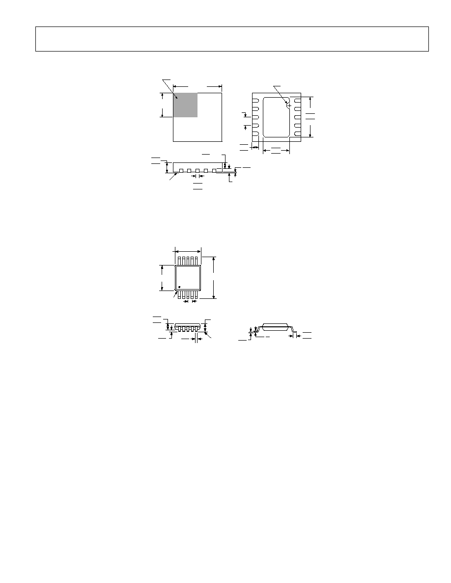
OUTLINE DIMENSIONS
3.00
BSC SQ
INDEX
AREA
TOP VIEW
1.50
BCS SQ
EXPOSED
PAD
(BOTTOM VIEW)
1.74
1.64
1.49
2.48
2.38
2.23
1
6
10
0.50
BSC
0.50
0.40
0.30
5
PIN 1
INDICATOR
0.80
0.75
0.70
0.05 MAX
0.02 NOM
SEATING
PLANE
0.30
0.23
0.18
0.20 REF
0.80 MAX
0.55 TYP
SIDE VIEW
Figure 44. . 10-Lead Lead Frame Chip Scale Package
(CP-10-9)
Dimensions shown in millimeters
0.23
0.08
0.80
0.60
0.40
8°
0°
0.15
0.00
0.27
0.17
0.95
0.85
0.75
SEATING
PLANE
1.10 MAX
10
6
5
1
0.50 BSC
3.00 BSC
3.00 BSC
4.90 BSC
PIN 1
COPLANARITY
0.10
COMPLIANT TO JEDEC STANDARDS MO-187BA
Figure 45. 10-Lead Mini Small Outline Package [MSOP]
(RM-10)
Dimensions shown in millimeters

AD5664
Preliminary Technical Data
Rev. PrA
| Page 26 of 28
ORDERING GUIDE
Model Temperature
Range
Package
Description
Package
Option Acurracy
AD5664ARMZ
-40°C to +105°C
10-lead MSOP
RM-10
±32 LSB INL
AD5664BRMZ
-40°C to +105°C
10-lead MSOP
RM-10
±16 LSB INL
AD5664BCPZ
-40°C to +105°C
10-lead LFCSP
CP-10
±16 LSB INL

Preliminary Technical Data
AD5664
Rev. PrA | Page 27 of 28
NOTES

AD5664
Preliminary Technical Data
Rev. PrA
| Page 28 of 28
NOTES
© 2005 Analog Devices, Inc. All rights reserved. Trademarks and
registered trademarks are the property of their respective owners.
PR05857-0-11/05(PrA)