AD5530/AD5531 Serial Input, Voltage Output 12-/14-Bit DACs Data Sheet (Rev. A)
Serial Input, Voltage Output
12-/14-Bit DACs
AD5530/AD5531
Rev. A
Information furnished by Analog Devices is believed to be accurate and reliable. However, no
responsibility is assumed by Analog Devices for its use, nor for any infringements of patents or other
rights of third parties that may result from its use. Specifications subject to change without notice. No
license is granted by implication or otherwise under any patent or patent rights of Analog Devices.
Trademarks and registered trademarks are the property of their respective owners.
One Technology Way, P.O. Box 9106, Norwood, MA 02062-9106, U.S.A.
Tel: 781.329.4700
www.analog.com
Fax: 781.461.3113
©2006 Analog Devices, Inc. All rights reserved.
FEATURES
Pin-compatible 12-, 14-bit DACs
Serial input, voltage output
Maximum output voltage range of ±10 V
Data readback
3-wire serial interface
Clear function to a user-defined voltage
Power-down function
Serial data output for daisy chaining
16-lead TSSOP
APPLICATIONS
Industrial automation
Automatic test equipment
Process control
General-purpose instrumentation
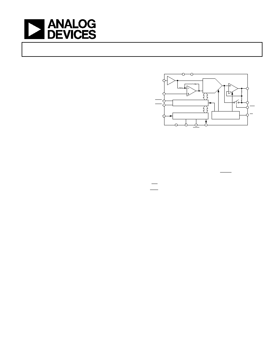
FUNCTIONAL BLOCK DIAGRAM
0
093
8-
001
LDAC
RBEN
REFAGND
SDIN
POWER-DOWN
CONTROL LOGIC
DAC REGISTER
REFIN
12-/14-BIT
DAC
R
R
GND
SCLK
SYNC
SDO
R
R
V
OUT
DUTGND
V
DD
V
SS
SHIFT REGISTER
AD5530/AD5531
CLR
PD
Figure 1.
GENERAL DESCRIPTION
The AD5530 and AD5531 are single 12-, 14-bit serial input,
voltage output DACs, respectively.
They utilize a versatile 3-wire interface that is compatible with
SPI®, QSPITM, MICROWIRETM, and DSP interface standards. Data
is presented to the part in the format of a 16-bit serial word.
Serial data is available on the SDO pin for daisy-chaining
purposes. Data readback allows the user to read the contents of
the DAC register via the SDO pin.
The DAC output is buffered by a gain of 2 amplifier and
referenced to the potential at DUTGND. LDAC can be used to
update the output of the DAC asynchronously. A power-down
(PD) pin allows the DAC to be put into a low power state, and a
CLR pin allows the output to be cleared to a user-defined
voltage, the potential at DUTGND.
The AD5530 and AD5531 are available in 16-lead TSSOP.

AD5530/AD5531
Rev. A | Page 2 of 20
TABLE OF CONTENTS
Features .............................................................................................. 1
Applications....................................................................................... 1
Functional Block Diagram .............................................................. 1
General Description ......................................................................... 1
Revision History ............................................................................... 2
Specifications..................................................................................... 3
AC Performance Characteristics ................................................ 5
Standalone Timing Characteristics............................................ 5
Daisy-Chaining and Readback Timing Characteristics.......... 6
Absolute Maximum Ratings............................................................ 7
ESD Caution.................................................................................. 7
Pin Configuration and Function Descriptions............................. 8
Terminology ...................................................................................... 9
Typical Performance Characteristics ........................................... 10
General Description ....................................................................... 13
DAC Architecture....................................................................... 13
Serial Interface ............................................................................ 13
PD Function................................................................................ 13
Readback Function .................................................................... 13
CLR Function.............................................................................. 13
Output Voltage............................................................................ 14
Bipolar Configuration................................................................ 14
Microprocessor Interfacing........................................................... 15
AD5530/AD5531 to ADSP-21xx.............................................. 15
AD5530/AD5531 to 8051 Interface ......................................... 15
AD5530/AD5531 to MC68HC11 Interface ............................ 15
Applications..................................................................................... 17
Optocoupler Interface................................................................ 17
Serial Interface to Multiple AD5530s or AD5531s ................ 17
Daisy-Chaining Interface with Multiple AD5530s or
AD5531s ...................................................................................... 17
Outline Dimensions ....................................................................... 18
Ordering Guide .......................................................................... 18
REVISION HISTORY
3/06--Rev. 0 to Rev. A
Change to Table 3 ............................................................................. 5
Change to Figure 4 ........................................................................... 8
Change to Output Voltage Section............................................... 14
Change to Ordering Guide............................................................ 18
2005--Revision 0: Initial Version

AD5530/AD5531
Rev. A | Page 3 of 20
SPECIFICATIONS
V
DD
= +15 V ± 10%; V
SS
= -15 V ± 10%; GND = 0 V; R
L
= 5 k and C
L
= 220 pF to GND. All specifications T
MIN
to T
MAX
, unless
otherwise noted.
Table 1.
Parameter
1
AD5530
AD5531
Unit
Test Conditions/Comments
ACCURACY
Resolution
12
14
Bits
Relative Accuracy
±1
±2
LSB max
Differential Nonlinearity
±1
±1
LSB max
Guaranteed monotonic over temperature
Zero-Scale Error
±2
±8
LSB max
Typically within ±1 LSB
Full-Scale Error
±2
±8
LSB max
Typically within ±1 LSB
Gain Error
±1
±4
LSB typ
Gain Temperature Coefficient
2
0.5
0.5
ppm FSR/°C typ
10
10
ppm FSR/°C max
REFERENCE INPUTS
2
Reference Input Range
0/5
0/5
V min/V max
Max output range ±10 V
DC Input Resistance
100
100
M typ
Input Current
±1
±1
A max
Per input, typically ±20 nA
DUTGND INPUT
2
DC Input Impedance
60
60
k typ
Max Input Current
±0.3
±0.3
mA typ
Input Range
-4/+4
-4/+4
V min/V max
Max output range ±10 V
O/P CHARACTERISTICS
2
Output Voltage Swing
±10
±10
V max
Short-Circuit Current
15
15
mA max
Resistive Load
5
5
k min
To 0 V
Capacitive Load
1200
1200
pF max
To 0 V
DC Output Impedance
0.5
0.5
max
DIGITAL I/O
V
INH
, Input High Voltage
2.4
2.4
V min
V
INL
, Input Low Voltage
0.8
0.8
V max
I
INH
, Input Current
±10
±10
A max
Total for all pins
C
IN
, Input Capacitance
2
10
10
pF max
3 pF typical
SDO V
OL
, Output Low Voltage
0.4
0.4
V max
I
SINK
= 1 mA
POWER REQUIREMENTS
V
DD
/V
SS
+15/-15
+15/-15
V nom
±10% for specified performance
Power Supply Sensitivity
Full Scale/V
DD
110
110
dB typ
Full Scale/V
SS
100
100
dB typ
I
DD
2
2
mA max
Outputs unloaded
I
SS
2
2
mA max
Outputs unloaded
I
DD
in Power-Down
150
150
A max
Typically 50 A
1
Temperature range for B Version: -40°C to +85°C.
2
Guaranteed by design, not subject to production test.
AD5530/AD5531
Rev. A | Page 4 of 20
V
DD
= +12 V ± 10%; V
SS
= -12 V ± 10%; GND = 0 V; R
L
= 5 k and C
L
= 220 pF to GND; T
A
= T
MIN
to T
MAX
, unless otherwise noted.
Table 2.
Parameter
1
AD5530
AD5531
Unit
Test Conditions/Comments
ACCURACY
Resolution
12
14
Bits
Relative Accuracy
±1
±2
LSB max
Differential Nonlinearity
±1
±1
LSB max
Guaranteed monotonic over temperature
Zero-Scale Error
±2
±8
LSB max
Typically within ±1 LSB
Full-Scale Error
±2
±8
LSB max
Typically within ±1 LSB
Gain Error
±1
±4
LSB typ
Gain Temperature Coefficient
2
0.5
0.5
ppm FSR/°C typ
10
10
ppm FSR/°C max
REFERENCE INPUTS
2
Reference Input Range
0/4.096
0/4.096
V min/V max
Max output range ±8.192 V
DC Input Resistance
100
100
M typ
Input Current
±1
±1
A max
Per input, typically ±20 nA
DUTGND INPUT
2
DC Input Impedance
60
60
k typ
Max Input Current
±0.3
±0.3
mA typ
Input Range
-3/+3
-3/+3
V min/V max
Max output range ±8.192 V
O/P CHARACTERISTICS
2
Output Voltage Swing
±8.192
±8.192
V max
Short-Circuit Current
15
15
mA max
Resistive Load
5
5
k min
To 0 V
Capacitive Load
1200
1200
pF max
To 0 V
DC Output Impedance
0.5
0.5
max
DIGITAL I/O
V
INH
, Input High Voltage
2.4
2.4
V min
V
INL
, Input Low Voltage
0.8
0.8
V max
I
INH
, Input Current
±10
±10
A max
Total for all pins
C
IN
, Input Capacitance
2
10
10
pF max
3 pF typical
SDO V
OL
, Output Low Voltage
0.4
0.4
V max
I
SINK
= 1 mA
POWER REQUIREMENTS
V
DD
/V
SS
+12/-12
+12/-12
V nom
±10% for specified performance
Power Supply Sensitivity
Full Scale/V
DD
110
110
dB typ
Full Scale/V
SS
100
100
dB typ
I
DD
2
2
mA max
Outputs unloaded
I
SS
2
2
mA max
Outputs unloaded
I
DD
in Power-Down
150
150
A max
Typically 50 A
1
Temperature range for B Version: -40°C to +85°C.
2
Guaranteed by design, not subject to production test.
AD5530/AD5531
Rev. A | Page 5 of 20
AC PERFORMANCE CHARACTERISTICS
V
DD
= 10.8 V to 16.5 V, V
SS
= -10.8 V to -16.5 V; GND = 0 V; R
L
= 5 k and C
L
= 220 pF to GND. All specifications T
MIN
to T
MAX
, unless
otherwise noted.
Table 3.
Parameter
B Version
Unit
Test Conditions/Comments
DYNAMIC PERFORMANCE
Output Voltage Settling Time
20
s typ
Full-scale change to ±½ LSB. DAC latch contents alternately
loaded with all 0s and all 1s.
Slew Rate
1.3
V/s typ
Digital-to-Analog Glitch Impulse
120
nV-s typ
DAC latch alternately loaded with 0FFF hex and 1000 hex. Not
dependent on load conditions.
Digital Feedthrough
0.5
nV-s typ
Effect of input bus activity on DAC output under test.
Output Noise Spectral Density @ 1 kHz
100
nV/Hz typ
All 1s loaded to DAC.
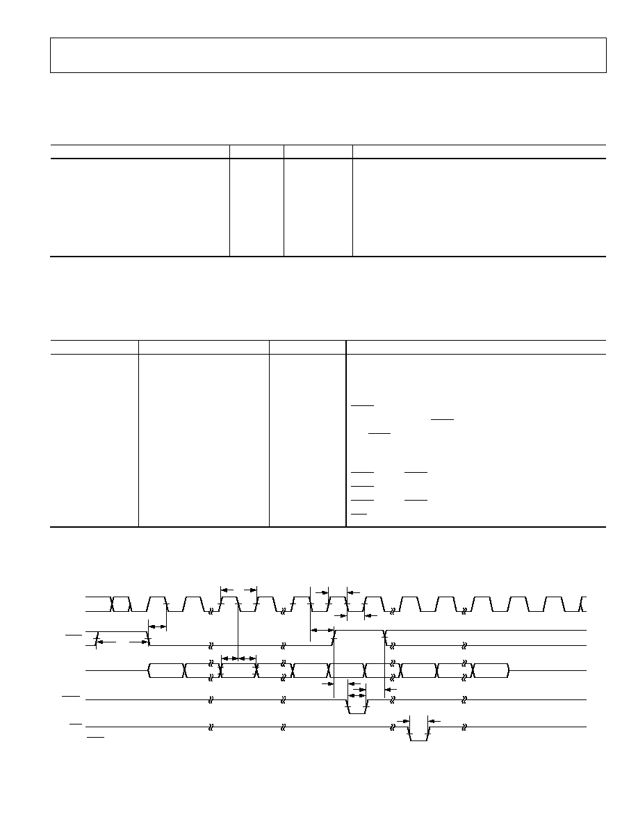
STANDALONE TIMING CHARACTERISTICS
V
DD
= 10.8 V to 16.5 V, V
SS
= -10.8 V to -16.5 V; GND = 0 V; R
L
= 5 k and C
L
= 220 pF to GND. All specifications T
MIN
to T
MAX
, unless
otherwise noted.
Table 4.
Parameter
1 , 2
Limit at T
MIN
, T
MAX
Unit
Description
f
MAX
7
MHz max
SCLK frequency
t
1
140
ns min
SCLK cycle time
t
2
60
ns min
SCLK low time
t
3
60
ns min
SCLK high time
t
4
50
ns min
SYNC to SCLK falling edge setup time
t
5
40
ns min
SCLK falling edge to SYNC rising edge
t
6
50
ns min
Min SYNC high time
t
7
40
ns min
Data setup time
t
8
15
ns min
Data hold time
t
9
5
ns min
SYNC high to LDAC low
t
10
50
ns min
LDAC pulse width
t
11
5
ns min
LDAC high to SYNC low
t
12
50
ns min
CLR pulse width
1
Guaranteed by design, not subject to production test.
2
Sample tested during initial release and after any redesign or process change that can affect this parameter. All input signals are measured with t
r
= t
f
= 5 ns (10% to
90% of V
DD
) and timed from a voltage level of (V
IL
+V
IH
)/2.
SCLK
SYNC
SDIN
MSB
DB15
DB14
DB11
DB0
LSB
t
1
t
3
t
2
t
5
t
4
t
6
t
7
t
8
t
9
t
10
t
11
t
12
LDAC
1
CLR
1
LDAC CAN BE TIED PERMANENTLY LOW, IF REQUIRED.
0
09
38
-
0
02
Figure 2. Timing Diagram for Standalone Mode
AD5530/AD5531
Rev. A | Page 6 of 20
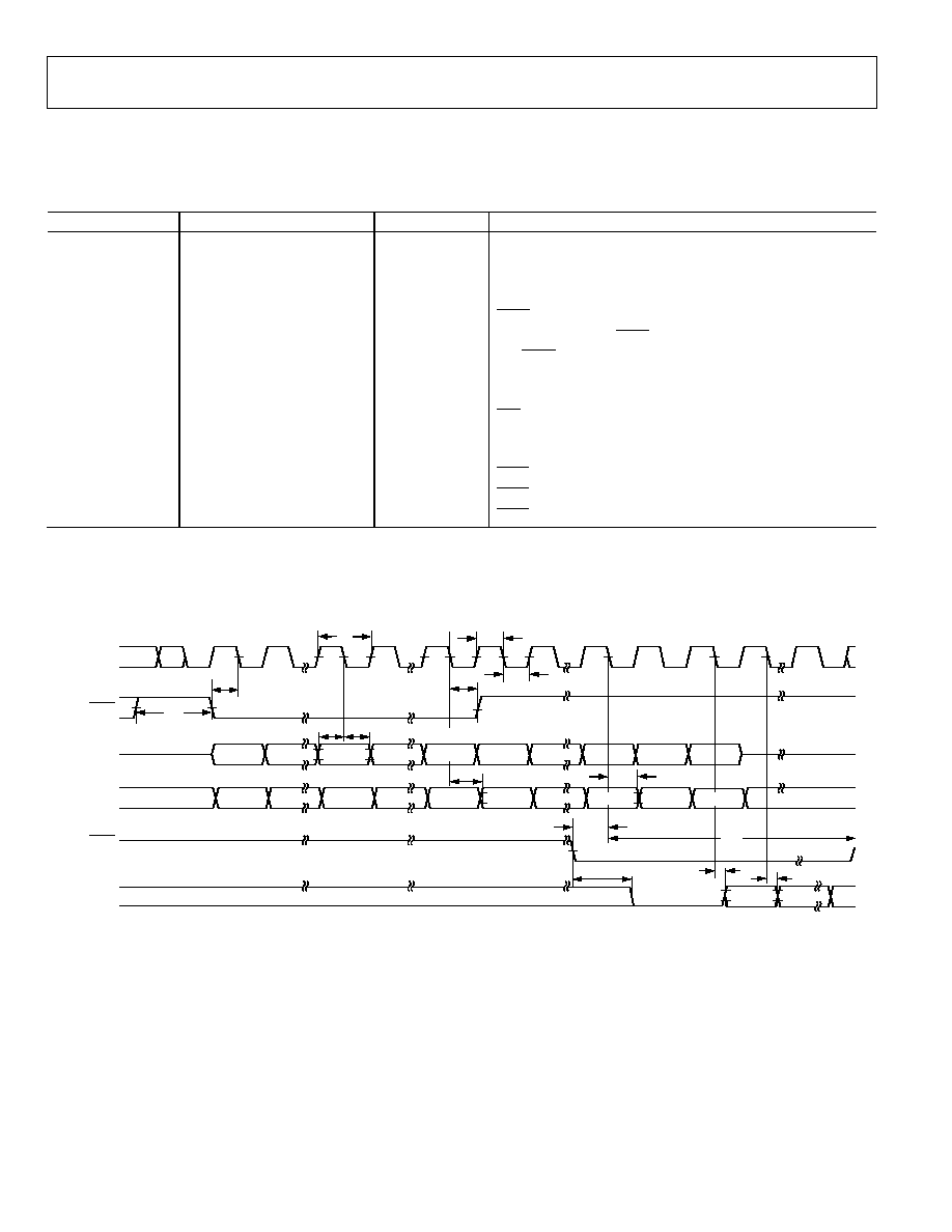
DAISY-CHAINING AND READBACK TIMING CHARACTERISTICS
V
DD
= 10.8 V to 16.5 V, V
SS
= -10.8 V to -16.5 V; V
SS
= -15 V ± 10%; GND = 0 V; R
L
= 5 k and C
L
= 220 pF to GND. All specifications
T
MIN
to T
MAX
, unless otherwise noted.
Table 5.
Parameter
1 , 2 , 3
Limit at T
MIN
, T
MAX
Unit
Description
f
MAX
2
MHz max
SCLK frequency
t
1
500
ns min
SCLK cycle time
t
2
200
ns min
SCLK low time
t
3
200
ns min
SCLK high time
t
4
50
ns min
SYNC to SCLK falling edge setup time
t
5
40
ns min
SCLK falling edge to SYNC rising edge
t
6
50
ns min
Min SYNC high time
t
7
40
ns min
Data setup time
t
8
15
ns min
Data hold time
t
12
50
ns min
CLR pulse width
t
13
130
ns min
SCLK falling edge to SDO valid
t
14
50
ns max
SCLK falling edge to SDO invalid
t
15
50
ns min
RBEN to SCLK falling edge setup time
t
16
50
ns min
RBEN hold time
t
17
100
ns min
RBEN falling edge to SDO valid
1
Guaranteed by design, not subject to production test.
2
Sample tested during initial release and after any redesign or process change that can affect this parameter. All input signals are measured with t
r
= t
f
= 5 ns (10% to
90% of V
DD
) and timed from a voltage level of (V
IL
+ V
IH
)/2.
3
SDO; R
PULLUP
= 5 k, C
L
= 15 pF
00938-
003
SCLK
SYNC
SDIN
SDO
(DAISY
CHAINING)
RBEN
SDO
(READBACK)
MSB
DB15
DB14
DB11
DB0
DB15
DB11
DB0
LSB
MSB
LSB
MSB
LSB
RB0
RB13
0
0
t
1
t
3
t
2
t
5
t
4
t
6
t
7
t
8
t
13
t
14
t
15
t
16
t
13
t
14
t
17
Figure 3. Timing Diagram for Daisy-Chaining and Readback Mode
AD5530/AD5531
Rev. A | Page 7 of 20
ABSOLUTE MAXIMUM RATINGS
T
A
= 25°C, unless otherwise noted.
Parameter Rating
V
DD
to GND
-0.3 V to +17 V
V
SS
to GND
+0.3 V to -17 V
Digital Inputs to GND
-0.3 V to V
DD
+ 0.3 V
SDO to GND
-0.3 V to +6.5 V
REFIN to REFAGND
-0.3 V to +17 V
REFIN to GND
V
SS
- 0.3 V to V
DD
+ 0.3 V
REFAGND to GND
V
SS
- 0.3 V to V
DD
+ 0.3 V
DUTGND to GND
V
SS
- 0.3 V to V
DD
+ 0.3 V
Operating Temperature Range
Industrial (B Version)
-40°C to +85°C
Storage Temperature Range
-65°C to +150°C
Maximum Junction Temperature (T
J MAX
) 150°C
Package Power Dissipation
(T
J MAX
T
A
)/
JA
Thermal Impedance
JA
TSSOP (RU-16)
150.4°C/W
Lead Temperature (Soldering 10 sec)
300°C
IR Reflow, Peak Temperature (<20 sec)
235°C
Stresses above those listed under Absolute Maximum Ratings
may cause permanent damage to the device. This is a stress
rating only; functional operation of the device at these or any
other conditions above those indicated in the operational
section of this specification is not implied. Exposure to absolute
maximum rating conditions for extended periods may affect
device reliability.
ESD CAUTION
ESD (electrostatic discharge) sensitive device. Electrostatic charges as high as 4000 V readily accumulate on
the human body and test equipment and can discharge without detection. Although this product features
proprietary ESD protection circuitry, permanent damage may occur on devices subjected to high energy
electrostatic discharges. Therefore, proper ESD precautions are recommended to avoid performance
degradation or loss of functionality.
AD5530/AD5531
Rev. A | Page 8 of 20
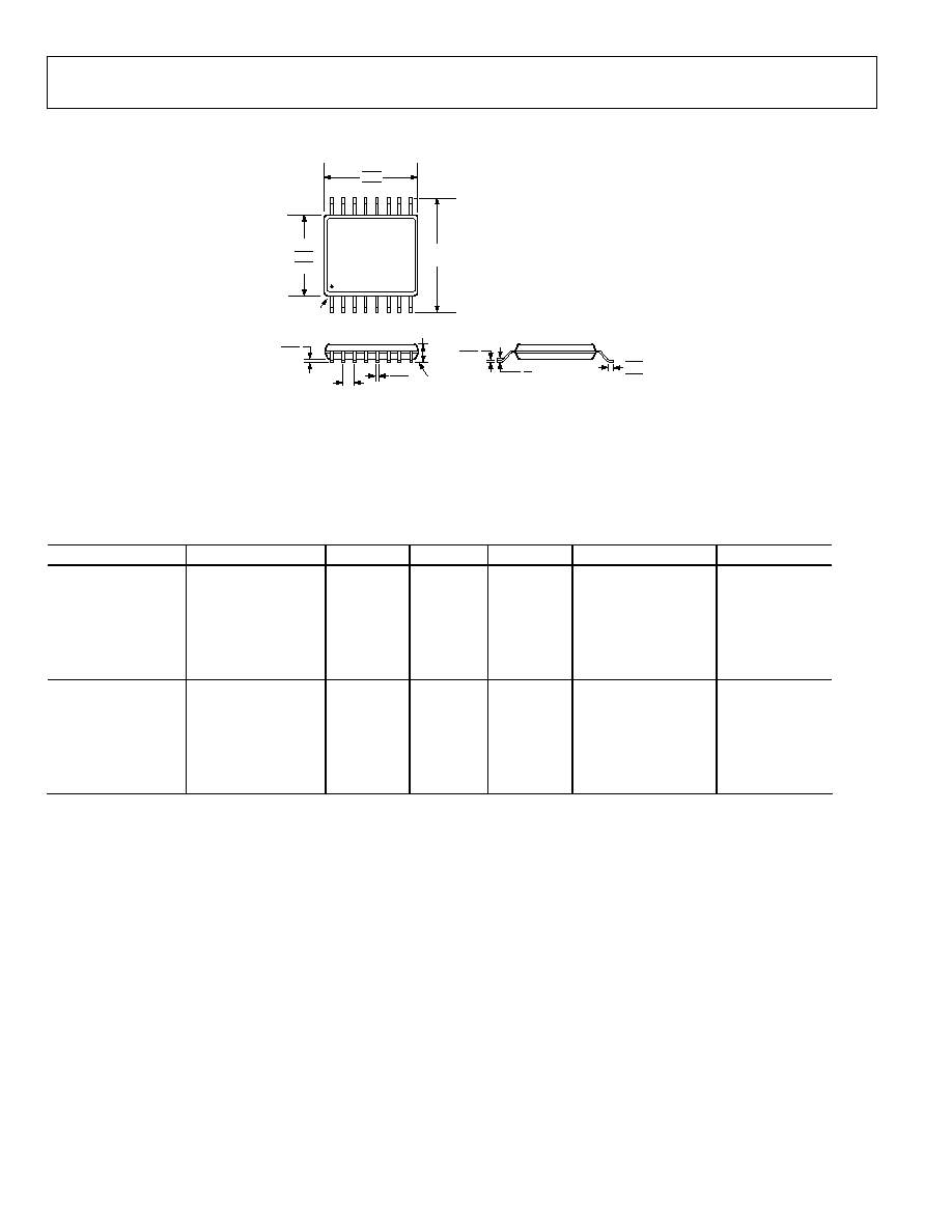
PIN CONFIGURATION AND FUNCTION DESCRIPTIONS
REFAGND
1
REFIN
2
LDAC
3
SDIN
4
SYNC
5
RBEN
6
SCLK
7
SDO
8
V
DD
16
V
OUT
15
DUTGND
14
V
SS
13
NC
12
GND
11
PD
10
CLR
9
AD5530/
AD5531
TOP VIEW
(Not to Scale)
NC = NO CONNECT
0
09
38
-
00
4
Figure 4. Pin Configuration
Table 6. Pin Function Descriptions
Pin Mnemonic Description
1
REFAGND
For bipolar ±10 V output range, this pin should be tied to 0 V.
2
REFIN
This is the voltage reference input for the DAC. Connect to external +5 V reference for specified bipolar ±10 V output.
3
LDAC
Load DAC Logic Input (Active Low). When taken low, the contents of the shift register are transferred to the DAC
register. LDAC can be tied permanently low enabling the outputs to be updated on the rising edge of SYNC.
4
SDIN
Serial Data Input. This device accepts 16-bit words. Data is clocked into the input register on the falling edge of SCLK.
5
SYNC
Active Low Control Input. Data is clocked into the shift requester on the falling edges of SCLK.
6
RBEN
Active Low Readback Enable Function. This function allows the contents of the DAC register to be read. Data from the
DAC register is shifted out on the SDO pin on each rising edge of SCLK.
7
SCLK
Clock Input. Data is clocked into the input register on the falling edge of SCLK.
8
SDO
Serial Data Out. This pin is used to clock out the serial data previously written to the input shift register or can be used
in conjunction with RBEN to read back the data from the DAC register. This is an open drain output; it should be pulled
high with an external pull-up resistor. In standalone mode, SDO should be tied to GND or left high impedance.
9
CLR
Level Sensitive, Active Low Input. A falling edge of CLR resets V
OUT
to DUTGND. The contents of the registers are
untouched.
10
PD
This allows the DAC to be put into a power-down state.
11
GND
Ground Reference.
12
NC
Do not connect anything to this pin.
13
V
SS
Negative Analog Supply Voltage. -12 V ± 10% or -15 V ± 10% for specified performance.
14
DUTGND
V
OUT
is referenced to the voltage applied to this pin.
15
V
OUT
DAC Output.
16
V
DD
Positive Analog Supply Voltage. +12 V ± 10% or +15 V ± 10% for specified performance.

AD5530/AD5531
Rev. A | Page 9 of 20
TERMINOLOGY
Relative Accuracy
Relative accuracy or endpoint linearity is a measure of the
maximum deviation, in LSBs, from a straight line passing
through the endpoints of the DAC transfer function.
Differential Nonlinearity
Differential nonlinearity is the difference between the measured
change and the ideal 1 LSB change between any two adjacent
codes. A specified differential nonlinearity of ±1 LSB maximum
ensures monotonicity.
Zero-Scale Error
Zero-scale error is a measure of the output error when all 0s are
loaded to the DAC latch.
Full-Scale Error
This is the error in DAC output voltage when all 1s are loaded
into the DAC latch. Ideally the output voltage, with all 1s loaded
into the DAC latch, should be 2 V
REF
- 1 LSB.
Gain Error
Gain error is the difference between the actual and ideal analog
output range, expressed as a percent of the full-scale range. It is
the deviation in slope of the DAC transfer characteristic from
ideal.
Output Voltage Settling Time
This is the amount of time it takes for the output to settle to a
specified level for a full-scale input change.
Digital-to-Analog Glitch Impulse
Digital-to-analog glitch impulse is the impulse injected into the
analog output when the input code in the DAC register changes
state. It is specified as the area of the glitch in nV-s and is
measured when the digital input code is changed by 1 LSB at
the major carry transition.
Digital Feedthrough
Digital feedthrough is a measure of the impulse injected into
the analog output of the DAC from the digital inputs of the
DAC, but is measured when the DAC output is not updated. It
is specified in nV-s and is measured with a full-scale code
change on the data bus, that is, from all 0s to all 1s and vice
versa.
AD5530/AD5531
Rev. A | Page 10 of 20
TYPICAL PERFORMANCE CHARACTERISTICS
1.0
1.0
0.8
0.6
0.4
0.2
0
0.2
0.4
0.6
0.8
0
500
1000
1500
2000
2500
3000
3500
4000
LS
B
CODE
00
93
8-
0
05
V
DD
= +15V
V
SS
= 15V
REFIN = +5V
REFAGND = 0V
T
A
= 25°C
Figure 5. AD5530 Typical INL Plot
0.5
0.5
0.4
0.3
0.2
0.1
0
0.1
0.2
0.3
0.4
0
500
1000
1500
2000
2500
3000
3500
4000
LS
B
CODE
00
93
8-
0
06
V
DD
= +15V
V
SS
= 15V
REFIN = +5V
REFAGND = 0V
T
A
= 25°C
Figure 6. AD5530 Typical DNL Plot
2.0
2.0
1.5
1.0
0.5
0
0.5
1.0
1.5
0
2000
4000
6000
8000
10000 12000 14000 16000
LS
B
CODE
00
93
8-
0
07
V
DD
= +15V
V
SS
= 15V
REFIN = +5V
REFAGND = 0V
T
A
= 25°C
Figure 7. AD5531 Typical INL Plot
1.00
1.00
0.75
0.50
0.25
0
0.25
0.50
0.75
0
2000
4000
6000
8000
10000 12000 14000 16000
LS
B
CODE
00
93
8-
0
08
V
DD
= +15V
V
SS
= 15V
REFIN = +5V
REFAGND = 0V
T
A
= 25°C
Figure 8. AD5531 Typical DNL Plot
2.0
2.0
1.5
1.0
0.5
0
0.5
1.0
1.5
40
80
60
40
20
0
20
E
RRO
R (
L
S
B
)
TEMPERATURE (°C)
00
93
8-
0
09
V
DD
= +15V
V
SS
= 15V
REFIN = +5V
REFAGND = 0V
Figure 9. AD5531 Typical INL Error vs. Temperature
1.0
1.0
0.8
0.6
0.2
0.4
0
0.2
0.4
0.6
0.8
40
80
60
40
20
0
20
E
RRO
R (
L
S
B
)
TEMPERATURE (°C)
00
93
8-
0
10
V
DD
= +15V
V
SS
= 15V
REFIN = +5V
REFAGND = 0V
Figure 10. AD5531 Typical DNL Error vs. Temperature
AD5530/AD5531
Rev. A | Page 11 of 20
3
2
1
3
2
1
0
2.0
6.0
5.5
5.0
4.5
4.0
3.5
3.0
2.5
E
RRO
R (
L
S
B
)
REFIN VOLTAGE (V)
00
93
8-
0
11
V
DD
= +15V
V
SS
= 15V
REFIN = 0V
T
A
= 25°C
NEGATIVE INL
POSITIVE INL
Figure 11. AD5531 Typical INL Error vs. Reference Voltage
0
2.5
2.0
1.5
1.0
0.5
40
20
0
20
40
60
80
E
RRO
R (
L
S
B
)
TEMPERATURE (°C)
00
93
8-
0
12
V
DD
= +15V
V
SS
= 15V
REFIN = +5V
REFAGND = 0V
Figure 12. Typical Full-Scale and Offset Error vs. Temperature
1.50
1.45
1.40
1.35
1.30
1.25
1.20
10
17
16
15
14
13
12
11
+85°C
+25°C
40°C
CUR
RE
NT
(
m
A)
V
DD
/V
SS
(V)
00
93
8-
01
3
Figure 13. I
DD
vs. V
DD
/V
SS
0.03
0.02
0.01
0
10
17
16
15
14
13
12
11
+85°C
+25°C
40°C
I
DD
(m
A
)
SUPPLY VOLTAGE (V)
00
93
8-
0
14
Figure 14. I
DD
in Power-Down vs. Supply
12
8
4
0
4
8
12
0
5
10
15
20
25
V
OU
T
(V
)
TIME (µs)
00
93
8-
0
15
V
DD
= +15V
V
SS
= 15V
REFIN = +5V
REFAGND = 0V
T
A
= 25°C
Figure 15. Settling Time
0
0.16
0.14
0.12
0.10
0.08
0.06
0.04
0.02
V
OU
T
(V
)
TIME (750ns/DIV)
00
93
8-
0
16
V
DD
= +15V
V
SS
= 15V
REFIN = +5V
REFAGND = 0V
T
A
= 25°C
Figure 16. Typical Digital-to-Analog Glitch Impulse
AD5530/AD5531
Rev. A | Page 12 of 20
0
09
38
-
0
17
V
OUT
2V/DIV
2V/DIV
PD
V
DD
= +15V
V
SS
= 15V
REFIN = +5V
REFAGND = 0V
T
A
= 25°C
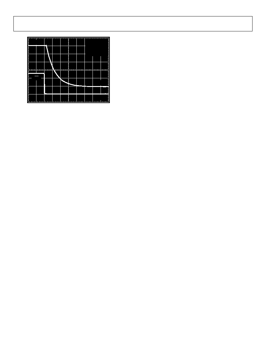
Figure 17. Typical Power-Down Time
AD5530/AD5531
Rev. A | Page 13 of 20
GENERAL DESCRIPTION
DAC ARCHITECTURE
The AD5530/AD5531 are pin-compatible 12-, 14-bit DACs.
The AD5530 consists of a straight 12-bit R-2R voltage mode
DAC, while the AD5531 consists of a 14-bit R-2R section. Using
a +5 V reference connected to the REFIN pin and REFAGND
tied to 0 V, a bipolar ±10 V voltage output results. The DAC
coding is straight binary.
SERIAL INTERFACE
Serial data on the SDIN input is loaded to the input register
under the control of SCLK, SYNC, and LDAC. A write
operation transfers a 16-bit word to the AD5530/AD5531.
Figure 2 and Figure 3 show the timing diagrams. Figure 18 and
Figure 19 show the contents of the input shift register. Twelve or
14 bits of the serial word are data bits; the rest are don't cares.
DB15 (MSB)
X X
D9
D10
D11
D8 D7 D6 D5 D4 D3 D2 D1 D0 X X
DB0 (LSB)
DATA BITS
00
93
8
-
01
8
Figure 18. AD5530 Input Shift Register Contents
X X
D11
D12
D13
D10 D9 D8 D7 D6 D5 D4 D3 D2 D1 D0
DB15 (MSB)
DB0 (LSB)
00
93
8-
01
9
DATA BITS
Figure 19. AD5531 Input Shift Register Contents
The serial word is framed by the signal, SYNC. After a high to
low transition on SYNC, data is latched into the input shift
register on the falling edges of SCLK. There are two ways in
which the DAC register and output can be updated. The LDAC
signal is examined on the falling edge of SYNC; depending on
its status, either a synchronous or asynchronous update is
selected. If LDAC is low, then the DAC register and output are
updated on the low to high transition of SYNC. Alternatively, if
LDAC is high upon sampling, the DAC register is not loaded
with the new data on a rising edge of SYNC. The contents of the
DAC register and the output voltage is updated by bringing
LDAC low any time after the 16-bit data transfer is complete.
LDAC can be tied permanently low if required. A simplified
diagram of the input loading circuitry is illustrated in Figure 20.
00
93
8-
02
0
SDO
LDAC
12-/14-BIT DAC
DAC REGISTER
SYNC REGISTER
16-BIT SHIFT
REGISTER
SYNC
SDIN
REFIN
14
14
14
OUTPUT
Figure 20. Simplified Serial Interface
Data written to the part via SDIN is available on the SDO Pin
16 clocks later if the readback function is not used. SDO data is
clocked out on the falling edge of the serial clock with some
delay.
PD FUNCTION
The PD pin allows the user to place the device into power-down
mode. While in this mode, power consumption is at a
minimum; the device draws only 50 A of current. The PD
function does not affect the contents of the DAC register.
READBACK FUNCTION
The AD5530/AD5531 allows the data contained in the DAC
register to be read back if required. The pins involved are the
RBEN and SDO (serial data out). When RBEN is taken low, on
the next falling edge of SCLK, the contents of the DAC register
are transferred to the shift register. RBEN can be used to frame
the readback data by leaving it low for 16 clock cycles, or it can
be asserted high after the required hold time. The shift register
contains the DAC register data and this is shifted out on the
SDO line on each falling edge of SCLK with some delay. This
ensures the data on the serial data output pin is valid for the
falling edge of the receiving part. The two MSBs of the 16-bit
word are 0s.
CLR FUNCTION
The falling edge of CLR causes V
OUT
to be reset to the same
potential as DUTGND. The contents of the registers remain
unchanged, so the user can reload the previous data with LDAC
after CLR is asserted high. Alternatively, if LDAC is tied low, the
output is loaded with the contents of the DAC register
automatically after CLR is brought high.
AD5530/AD5531
Rev. A | Page 14 of 20
OUTPUT VOLTAGE
The DAC transfer function is as follows:
(
)
DUTGND
REFIN
REFAGND
D
REFAGND
REFIN
V
N
OUT
-
-
×
+
×
-
×
×
=
2
2
2
2
where:
D is the decimal data word loaded to the DAC register.
N is the resolution of the DAC.
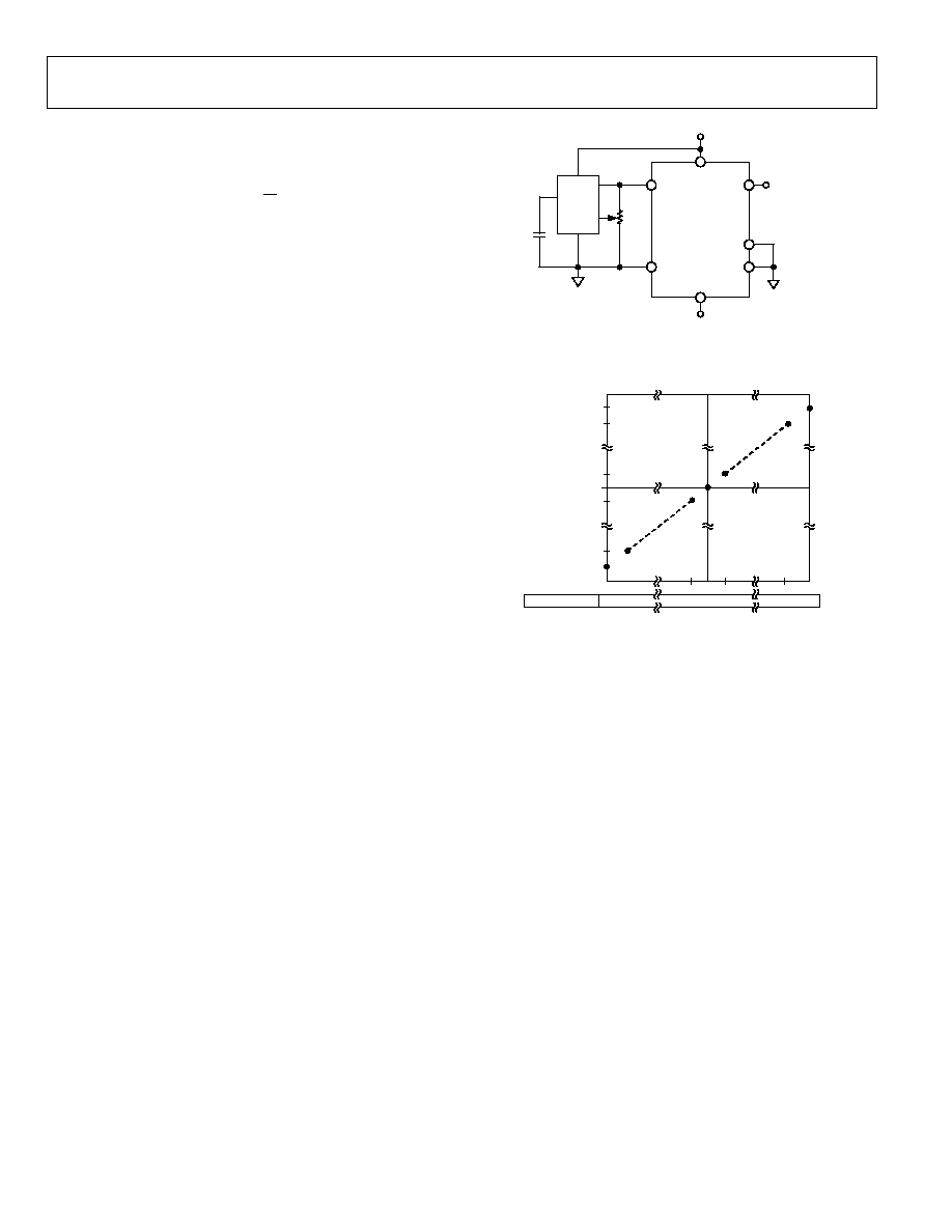
BIPOLAR CONFIGURATION
Figure 21 shows the AD5530/AD5531 in a bipolar circuit
configuration. REFIN is driven by the AD586, 5 V reference,
while the REFAGND and DUTGND pins are tied to GND. This
results in a bipolar output voltage ranging from -10 V to +10 V.
Resistor R1 is provided (if required) for gain adjust. Figure 22
shows the transfer function of the DAC when REFAGND is tied
to 0 V.
0
09
38
-
02
1
C1
1µF
R1
10k
9
2
6
+15V
V
OUT
V
OUT
DUTGND
GND
SIGNAL
GND
SIGNAL
GND
1
ADDITIONAL PINS OMITTED FOR CLARITY.
V
OUT
(10V TO +10V)
REFIN
REFAGND
AD5530/
AD5531
1
V
SS
15V
5
4
AD586
Figure 21. Bipolar ±10 V Operation
009
38
-
02
2
2 REFIN
2 REFIN
DAC INPUT CODE 000 001
(3)FFF
DAC O
UT
P
UT
V
O
L
T
AG
E
0V
Figure 22. Output Voltage vs. DAC Input Codes (Hex)
AD5530/AD5531
Rev. A | Page 15 of 20
MICROPROCESSOR INTERFACING
Microprocessor interfacing to the AD5530/AD5531 is via a
serial bus that uses standard protocol compatible with
microcontrollers and DSP processors. The communications
channel is a 3-wire (minimum) interface consisting of a clock
signal, a data signal, and a synchronization signal. The
AD5530/AD5531 requires a 16-bit data word with data valid on
the falling edge of SCLK.
For all the interfaces, the DAC output update can be done
automatically when all the data is clocked in or asynchronously
under the control of LDAC.
The contents of the DAC register can be read using the
readback function. RBEN is used to frame the readback data,
which is clocked out on SDO. The following figures illustrate
these DACs interfacing with a simple 4-wire interface. The
serial interface of the AD5530/AD5531 can be operated from a
minimum of three wires.
AD5530/AD5531 TO ADSP-21xx
An interface between the AD5530/AD5531 and the ADSP-21xx
is shown in Figure 23. In the interface example shown, SPORT0
is used to transfer data to the DAC. The SPORT control register
should be configured as follows: internal clock operation,
alternate framing mode; active low framing signal.
Transmission is initiated by writing a word to the Tx register
after the SPORT has been enabled. As the data is clocked out of
the DSP on the rising edge of SCLK, no glue logic is required to
interface the DSP to the DAC. In the interface shown, the DAC
output is updated using the LDAC pin via the DSP. Alternatively,
the LDAC input could be tied permanently low and then the
update takes place automatically when TFS is taken high.
AD5530/
AD5531
1
ADSP-2101/
ADSP-2103
1
1
ADDITIONAL PINS OMITTED FOR CLARITY.
LDAC
FO
SYNC
TFS
SDIN
DT
SCLK
SCLK
00
93
8-
0
23
Figure 23. AD5530/AD5531 to ADSP-21xx Interface
AD5530/AD5531 TO 8051 INTERFACE
A serial interface between the AD5530/AD5531 and the 8051 is
shown in Figure 24. TxD of the 8051 drives SCLK of the
AD5530/AD5531, while RxD drives the serial data line, SDIN.
P3.3 and P3.4 are bit-programmable pins on the serial port and
are used to drive SYNC and LDAC respectively.
The 8051 provides the LSB of its SBUF register as the first bit in
the data stream. The user has to ensure that the data in the
SBUF register is arranged correctly as the DAC expects
MSB first.
AD5530/
AD5531
1
80C51/80L51
1
1
ADDITIONAL PINS OMITTED FOR CLARITY.
LDAC
P3.4
SYNC
P3.3
SDIN
RxD
SCLK
TxD
00
93
8-
0
24
Figure 24. AD5530/AD5531 to 8051 Interface
When data is to be transmitted to the DAC, P3.3 is taken low.
Data on RxD is clocked out of the microcontroller on the rising
edge of TxD and is valid on the falling edge. As a result no glue
logic is required between this DAC and microcontroller
interface.
The 8051 transmits data in 8-bit bytes with only eight falling
clock edges occurring in the transmit cycle. As the DAC expects
a 16-bit word, P3.3 must be left low after the first 8 bits are
transferred. After the second byte has been transferred, the P3.3
line is taken high. The DAC can be updated using LDAC via
P3.4 of the 8051.
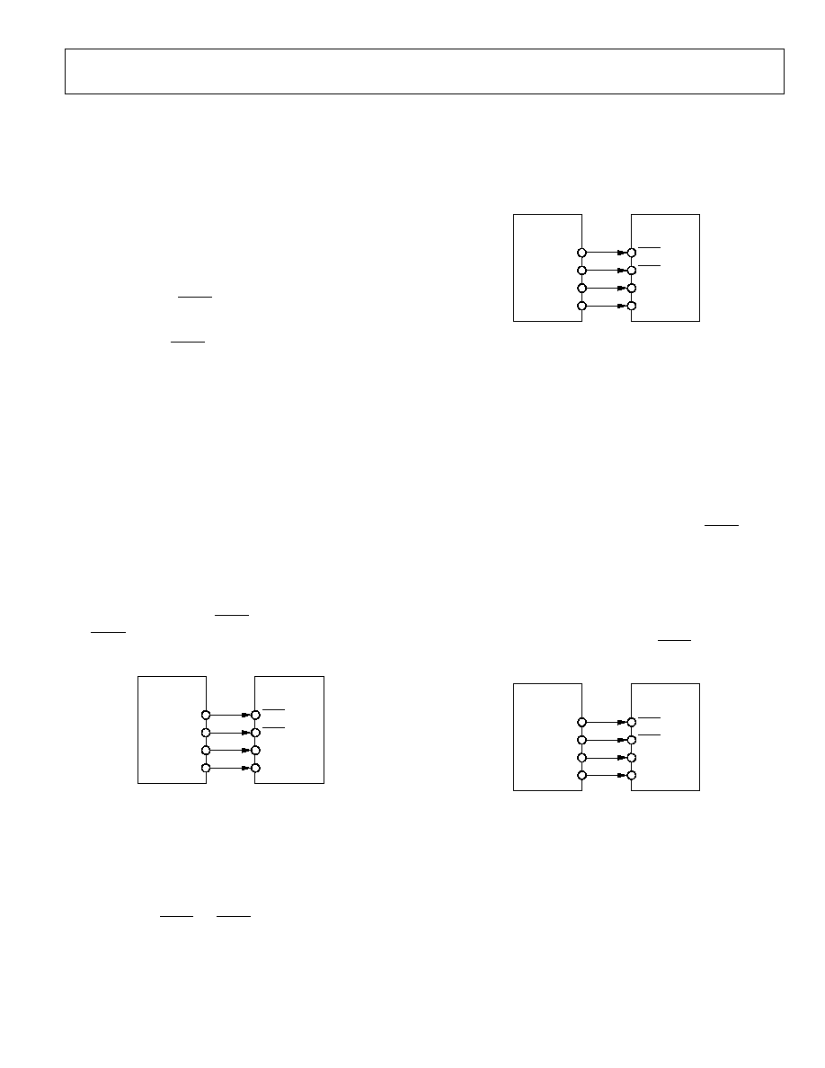
AD5530/AD5531 TO MC68HC11 INTERFACE
Figure 25 shows an example of a serial interface between the
AD5530/AD5531 and the MC68HC11 microcontroller. SCK of
the 68HC11 drives the SCLK of the DAC, while the MOSI
output drives the serial data lines, SDIN. SYNC is driven from
one of the port lines, in this case PC7.
AD5530/
AD5531
1
MC68HC11
1
1
ADDITIONAL PINS OMITTED FOR CLARITY.
LDAC
PC6
SYNC
PC7
SDIN
MOSI
SCLK
SCK
00
93
8-
0
25
Figure 25. AD5530/AD5531 to MC68HC11 Interface
The 68HC11 is configured for master mode, MSTR = 1,
CPOL = 0, and CPHA = 1. When data is transferred to the part,
PC7 is taken low and data is transmitted MSB first. Data
appearing on the MOSI output is valid on the falling edge of
SCK. Eight falling clock edges occur in the transmit cycle, so to
load the required 16-bit word, PC7 is not brought high until the
second 8-bit word has been transferred to the DAC's input shift
register.

AD5530/AD5531
Rev. A | Page 16 of 20
LDAC is controlled by the PC6 port output. The DAC can be
updated after each 2-byte transfer by bringing LDAC low. This
example does not show other serial lines for the DAC. If CLR
were used, it could be controlled by port output PC5. To read
data back from the DAC register, the SDO line can be
connected to MISO of the MC68HC11, with RBEN tied to
another port output controlling and framing the readback
data transfer.
AD5530/AD5531
Rev. A | Page 17 of 20
APPLICATIONS
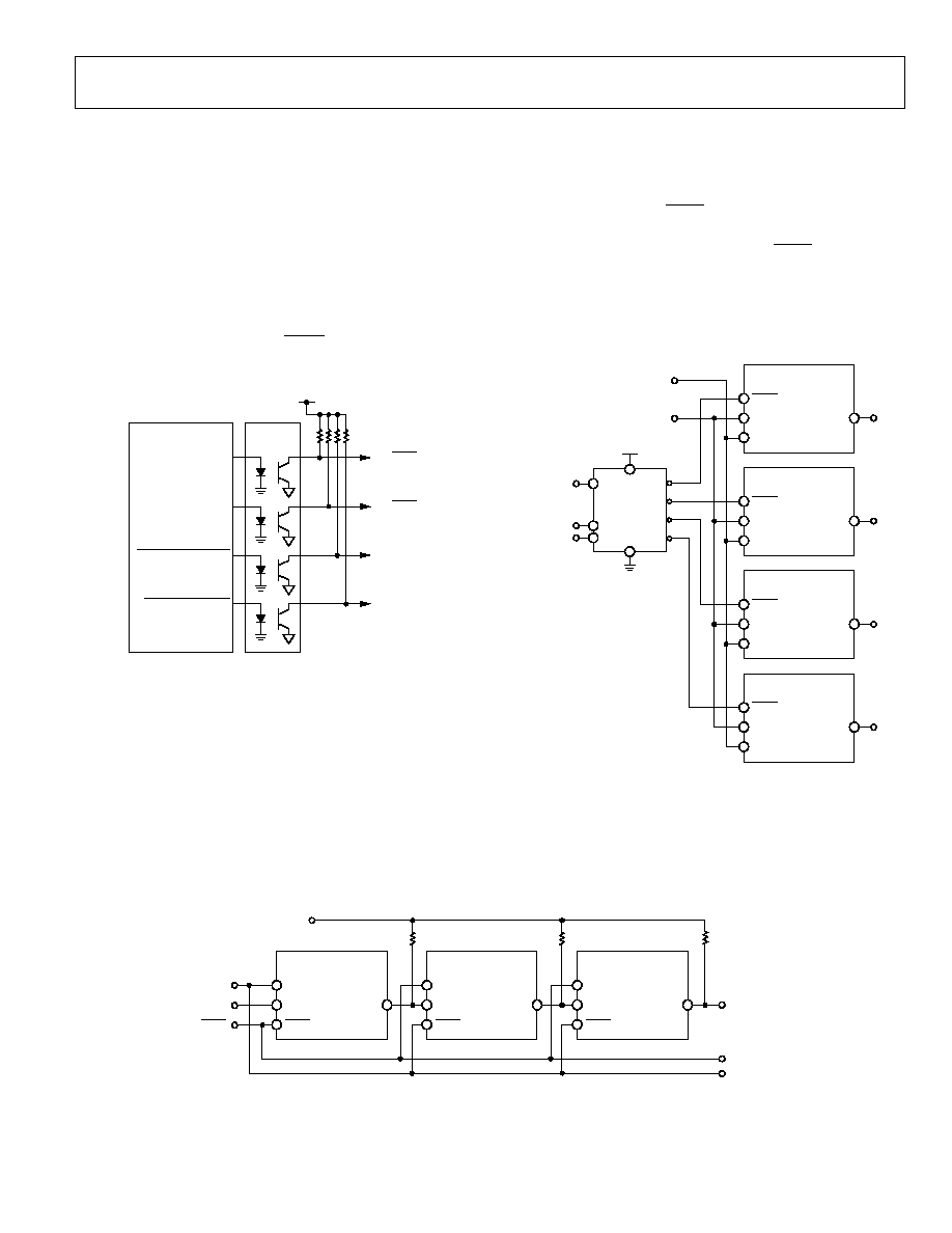
OPTOCOUPLER INTERFACE
In many process control applications, it is necessary to provide
an isolation barrier between the controller and the unit being
controlled. Opto-isolators can provide voltage isolation in
excess of 3 kV. The serial loading structure of the AD5530/
AD5531 makes it ideal for opto-isolated interfaces as the
number of interface lines is kept to a minimum. Figure 26
shows a 4-channel isolated interface to the AD5530/AD5531.
To reduce the number of opto-isolators, if simultaneous
updating is not required, then the LDAC pin can be tied
permanently low.
00
93
8-
02
6
µCONTROLLER
CONTROL OUT
TO LDAC
SYNC OUT
TO SYNC
SERIAL CLOCK OUT
TO SCLK
SERIAL DATA OUT
TO SDIN
OPTOCOUPLER
V
CC
Figure 26. Opto-Isolated Interface
SERIAL INTERFACE TO MULTIPLE AD5530S OR
AD5531S
Figure 27 shows how the SYNC pin is used to address multiple
AD5530/AD5531s. All devices receive the same serial clock and
serial data, but only one device receives the SYNC signal at any
one time. The DAC addressed is determined by the decoder.
There is some feedthrough from the digital input lines, the
effects of which can be minimized by using a burst clock.
00
93
8-
0
27
AD5530/AD5531
1
V
OUT
SYNC
SDIN
SCLK
AD5530/AD5531
1
V
OUT
SYNC
SDIN
SCLK
AD5530/AD5531
1
V
OUT
SYNC
SDIN
SCLK
AD5530/AD5531
1
V
OUT
SYNC
SDIN
SCLK
SCLK
SDIN
V
CC
DECODER
1
ENABLE
EN
CODED
ADDRESS
DGND
1
ADDITIONAL PINS
OMITTED FOR CLARITY.
Figure 27. Addressing Multiple AD5530/AD5531s
DAISY-CHAINING INTERFACE WITH MULTIPLE AD5530S OR AD5531S
A number of these DAC parts can be daisy-chained together using the SDO pin. Figure 28 illustrates such a configuration.
0
09
38
-
02
8
AD5530/AD5531
1
SDO
SCLK
SDIN
SYNC
SCLK
SDIN
SYNC
AD5530/AD5531
1
SDO
SCLK
SDIN
SYNC
AD5530/AD5531
1
SDO
SCLK
SDIN
SYNC
TO OTHER
SERIAL DEVICES
V
DD
R
R
R
1
ADDITIONAL PINS OMITTED FOR CLARITY.
Figure 28. Daisy-Chaining Multiple AD5530/AD5531s
AD5530/AD5531
Rev. A | Page 18 of 20
OUTLINE DIMENSIONS
16
9
8
1
PIN 1
SEATING
PLANE
8°
0°
4.50
4.40
4.30
6.40
BSC
5.10
5.00
4.90
0.65
BSC
0.15
0.05
1.20
MAX
0.20
0.09
0.75
0.60
0.45
0.30
0.19
COPLANARITY
0.10
COMPLIANT TO JEDEC STANDARDS MO-153-AB
Figure 29. 16-Lead Thin Shrink Small Outline Package (TSSOP)
(RU-16)
Dimensions shown in millimeters
ORDERING GUIDE
Model
Temperature Range Resolution
INL (LSBs)
DNL (LSBs)
Package Description
Package Option
AD5530BRU
-40°C to +85°C
12
±1
±1
16-Lead TSSOP
RU-16
AD5530BRU-REEL
-40°C to +85°C
12
±1
±1
16-Lead TSSOP
RU-16
AD5530BRU-REEL7
-40°C to +85°C
12
±1
±1
16-Lead TSSOP
RU-16
AD5530BRUZ
1
-40°C to +85°C
12
±1
±1
16-Lead TSSOP
RU-16
AD5530BRUZ-REEL
1
-40°C to +85°C
12
±1
±1
16-Lead TSSOP
RU-16
AD5530BRUZ-REEL7
1
-40°C to +85°C
12
±1
±1
16-Lead TSSOP
RU-16
AD5531BRU
-40°C to +85°C
14
±2
±1
16-Lead TSSOP
RU-16
AD5531BRU-REEL
-40°C to +85°C
14
±2
±1
16-Lead TSSOP
RU-16
AD5531BRU-REEL7
-40°C to +85°C
14
±2
±1
16-Lead TSSOP
RU-16
AD5531BRUZ
1
-40°C to +85°C
14
±2
±1
16-Lead TSSOP
RU-16
AD5531BRUZ-REEL
1
-40°C to +85°C
14
±2
±1
16-Lead TSSOP
RU-16
AD5531BRUZ-REEL7
1
-40°C to +85°C
14
±2
±1
16-Lead TSSOP
RU-16
1
Z = Pb-free part.

AD5530/AD5531
Rev. A | Page 19 of 20
NOTES

AD5530/AD5531
Rev. A | Page 20 of 20
NOTES
©2006 Analog Devices, Inc. All rights reserved. Trademarks and
registered trademarks are the property of their respective owners.
C00938-0-3/06(A)
Document Outline
- þÿ
- þÿ
- þÿ
- þÿ
- þÿ
- þÿ
- þÿ
- þÿ
- þÿ
- þÿ
- þÿ
- þÿ
- þÿ
- þÿ
- PD FUNCTION
- þÿ
- CLR FUNCTION
- OUTPUT VOLTAGE
- þÿ
- þÿ
- þÿ
- þÿ
- SERIAL INTERFACE TO MULTIPLE AD5530S OR AD5531S
- þÿ
- þÿ