 | ÐлекÑÑоннÑй компоненÑ: AD53509 | СкаÑаÑÑ:  PDF PDF  ZIP ZIP |
Äîêóìåíòàöèÿ è îïèñàíèÿ www.docs.chipfind.ru
REV. A
Information furnished by Analog Devices is believed to be accurate and
reliable. However, no responsibility is assumed by Analog Devices for its
use, nor for any infringements of patents or other rights of third parties
which may result from its use. No license is granted by implication or
otherwise under any patent or patent rights of Analog Devices.
a
AD53509
One Technology Way, P.O. Box 9106, Norwood, MA 02062-9106, U.S.A.
Tel: 781/329-4700
World Wide Web Site: http://www.analog.com
Fax: 781/326-8703
© Analog Devices, Inc., 2000
High-Performance Driver/Comparator
Active Load on a Single Chip
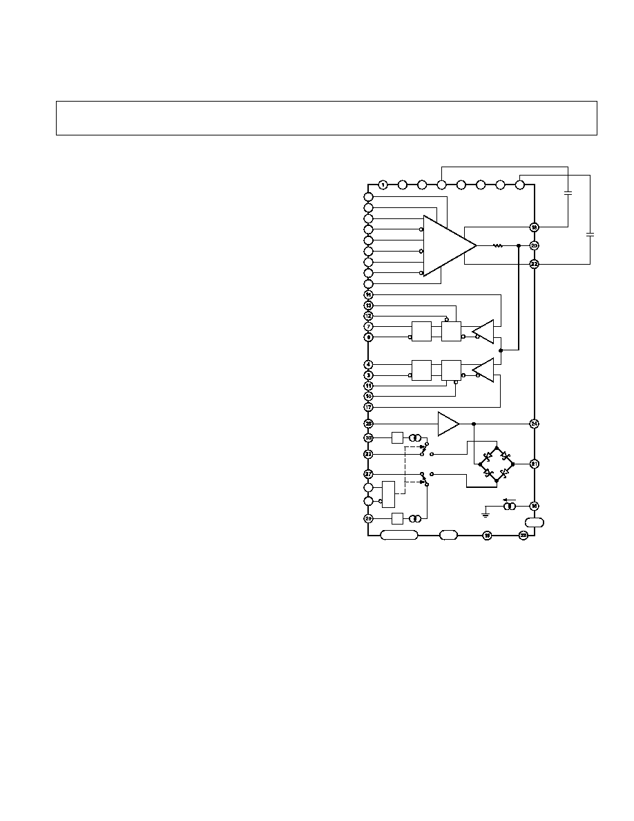
FUNCTIONAL BLOCK DIAGRAM
DRIVER
COMPARATOR
46
V/I
V/I
ACTIVE LOAD
1.0 A/K
V
CC
V
CC
V
CC
34
V
CC
V
EE
V
EE
V
EE
V
EE
51
52
39
40
41
32
AD53509
VHDCPL
V
OUT
VLDCPL
39nF
CHDCPL
39nF
CLDCPL
2,5,8
9,33,44,46,48
PWRGND
VCCO
HQGND2
HQGND
VCOMS
THERM
NC
35
36
+1
31
50
49
42
43
38
37
45
47
VH
VTERM
DATA
DATA
IOD
IOD
RLD
RLD
V
L
HCOMP
LEH
LEH
QH
QH
QL
QL
LEL
LEL
LCOMP
VCOMI
IOLC
IOLRTN
IOHRTN
INHL
INHL
IOHC
NC = NO CONNECT
OUT_L
14, 26
FEATURES
250 MHz Operation
Driver/Comparator and Active Load Included
On-Chip Schottky Diode Bridge
52-Lead LQFP Package with Built-In Heat Sink
APPLICATIONS
Automatic Test Equipment
Semiconductor Test Systems
Board Test Systems
Instrumentation and Characterization Equipment
PRODUCT DESCRIPTION
The AD53509 is a single chip that performs the pin electronics
functions of driver, comparator and active load in ATE VLSI
and memory testers. In addition, a Schottky diode bridge for the
active load and a VCOM buffer are included internally.
The driver is a proprietary design that features three active
states: Data High Mode, Data Low Mode and Term Mode as
well as an Inhibit State. This facilitates the implementation of
high speed active termination. The output voltage range is 2 V
to +7 V to accommodate a wide variety of test devices. The
output leakage is typically less than 250 nA over the entire sig-
nal range.
The dual comparator, with an input range equal to the driver
output range, features built-in latches and ECL-compatible
outputs. The outputs are capable of driving 50
signal lines
terminated to 2 V. Signal tracking capability is upwards of
5 V/ns.
The active load can be set for up to 40 mA load current with
less than a 10
µA linearity error through the entire set range.
I
OH
, I
OL
and the buffered VCOM are independently adjustable.
On-board Schottky diodes provide high speed switching and low
capacitance.
Also included on the chip is an on-board temperature sensor
whose purpose is to give an indication of the surface tempera-
ture of the DCL. This information can be used to measure
JC
and
JA
or flag an alarm if proper cooling is lost. Output from
the sensor is a current sink that is proportional to absolute tem-
perature. The gain is trimmed to a nominal value of 1.0
µA/K.
As an example, the output current can be sensed by using a
10 k
resistor connected from 10 V to the THERM (IOUT) pin.
A voltage drop across the resistor will be developed that equals:
10K
× 1 µA/K = 10 mV/K = 2.98 V at room temperature.
2
REV. A
AD53509SPECIFICATIONS
DRIVER SPECIFICATIONS
(All specifications are at T
J
= 85 C
5 C, V
S
= 11 V
3%, V
S
= 6 V = 3% unless otherwise noted. All temperature coefficients are
measured at T
J
= 75 C to 95 C.)
Parameter
Min
Typ
Max
Unit
Test Conditions
DIFFERENTIAL INPUT CHARACTERISTICS
(DATA to
DATA, IOD to IOD, RLD to RLD)
Input Voltage
2
+3
V
Differential Input Range
2
V
All Digital Inputs Within a 2 V Range
Bias Current
250
+250
µA
V
IN
= 2 V, +3 V
REFERENCE INPUTS
Bias Currents
50
+50
µA
V
L
, V
H
, V
T
= 5 V
OUTPUT CHARACTERISTICS
Logic High Range
2
+7
V
DATA = H, V
H
= 2 V to +7 V, V
L
= 2 V, V
T
= 0 V
Logic Low Range
2
+6
V
DATA = L, V
L
= 2 V to +6 V, V
H
= 7 V, V
T
= 0 V
Amplitude (V
H
and V
L
)
0.1
9
V
V
L
= 0.0 V, V
H
= 0.1 V, V
T
= 0 V
Absolute Accuracy
V
L
= 2 V, V
H
= +7 V, V
T
= 0 V
V
H
Offset
50
+50
mV
DATA = H, V
H
= 0 V, V
L
= 2 V, V
T
= 1 V
V
H
Gain + Linearity Error
0.3 5
+0.3 + 5
% of V
H
+ mV
DATA = H, V
H
= 1 V to +7 V, V
L
= 2 V, V
T
= 2 V
V
L
Offset
50
+50
mV
DATA = L, V
L
= 0 V, V
H
= 5 V, V
T
= 3 V
V
L
Gain + Linearity Error
0.3 5
+0.3 + 5
% of V
L
+ mV
DATA = L, V
L
= 2 V to +6 V, V
H
= 7 V, V
T
= 7 V
Offset TC
0.5
mV/
°C
V
L
= 2 V, V
H
= 0 V, V
T
= 1 V (V
H
Offset)
V
L
= 0 V, V
H
= 5 V, V
T
= 3 V (V
L
Offset)
Output Resistance
V
H
= 2 V
44
46
48
V
L
= 2 V, V
T
= 0 V, I
OUT
= 0, +1, +30 mA
V
H
= +7 V
44
46
48
V
L
= 1 V, V
T
= 0 V, I
OUT
= 0, 1, 30 mA
V
L
= 2 V
44
46
48
V
H
= 6 V, V
T
= 0 V, I
OUT
= 0, 1, 30 mA
V
L
= +6 V
44
46
48
V
H
= 7 V, V
T
= 0 V, I
OUT
= 0, 1, 30 mA
V
H
= +3 V
46
V
L
= 0 V, V
T
= 0 V, I
OUT
= 30 mA (Trim Point)
Dynamic Current Limit
>100
mA
C
BYP
= 39 nF, V
H
= 6 V, V
L
= 2 V, V
T
= 0 V
Static Current Limit
85
+85
mA
Output to 2 V, V
H
= 7 V, V
L
= 1 V, V
T
= 0 V
DATA = H and Output to 7 V, V
H
= 6 V,
V
L
= 2 V, V
T
= 0 V, DATA = L
V
T
ERM
Voltage Range
2
+7
V
TERM MODE, V
T
= 2 V to +7 V, V
L
= 0 V, V
H
= 3 V
V
T
ERM
Offset
50
+50
mV
TERM MODE, V
T
= 0 V, V
L
= 0 V, V
H
= 3 V
V
T
ERM
Gain + Linearity Error
0.3 +10
+0.3 +10 % of V
SET
+ mV
TERM MODE, V
T
= 2 V to +7 V, V
L
= 0 V, V
H
= 3 V
Offset TC
0.5
mV/
°C
V
T
= 0 V, V
L
= 0 V, V
H
= 3 V
Output Resistance
44
46
49
I
OUT
= +30 mA, +1.0 mA, V
T
= 2.0 V, V
H
= 3 V, V
L
= 0 V
I
OUT
= 30 mA, 1.0 mA, V
T
= +7.0 V, V
H
= 3 V, V
L
= 0 V
I
OUT
=
±30 mA, ±1.0 mA, V
T
= 0 V, V
H
= 3 V, V
L
= 0 V
DYNAMIC PERFORMANCE, (V
H
AND V
L
)
Propagation Delay Time
1.5
ns
Measured at 50%, V
H
= +400 mV, V
L
= 400 mV,
V
T
= 0 V
Propagation Delay TC
2
ps/
°C
Measured at 50%, V
H
= +400 mV, V
L
= 400 mV,
V
T
= 0 V
Delay Matching, Edge to Edge
<100
ps
Measured at 50%, V
H
= +400 mV, V
L
= 400 mV,
V
T
= 0 V
Rise and Fall Times
1 V Swing
0.42
ns
Measured 20%80%, V
L
= 0 V, V
H
= 1 V, V
T
= 0 V
3 V Swing
0.75
ns
Measured 20%80%, V
L
= 0 V, V
H
= 3 V, V
T
= 0 V
5 V Swing
1.65
ns
Measured 10%90%, V
L
= 0 V, V
H
= 5 V, V
T
= 0 V
9 V Swing
3.0
ns
Measured 10%90%, V
L
= 2 V, V
H
= 7 V, V
T
= 0 V
Rise and Fall Time Temperature Coefficient
1 V Swing
±1
ps/
°C
Measured 20%80%, V
L
= 0 V, V
H
= 1 V
3 V Swing
±2
ps/
°C
Measured 20%80%, V
L
= 0 V, V
H
= 3 V
5 V Swing
±4
ps/
°C
Measured 10%90%, V
L
= 0 V, V
H
= 5 V
Overshoot and Preshoot
<3 + 50
% of Step + mV
V
L
, V
H
= 0.1 V, 0.1 V, V
L
, V
H
= 0.0 V, 1.0 V
V
L
, V
H
= 0.0 V, 3.0 V, V
L
, V
H
= 0.0 V, 5.0 V
V
L
, V
H
= 2.0 V, 7.0 V
Settling Time
to 15 mV
<50
ns
V
L
= 0 V, V
H
= 0.5 V, V
T
= 2 V
to 4 mV
<10
µs
V
L
= 0 V, V
H
= 0.5 V, V
T
= 2 V
3
REV. A
AD53509
Parameter
Min
Typ
Max
Unit
Test Conditions
Delay Change vs. Pulsewidth
50
ps
V
L
= 0 V, V
H
= 2 V, Pulsewidth = 2.5 ns/7.5 ns, 30 ns/90 ns
Minimum Pulsewidth
3 V Swing
1.4
ns
V
L
= 0 V, V
H
= 3 V, 90% (2.7 V) Reached, Measure @ 50%
5 V Swing
2.0
ns
V
L
= 0 V, V
H
= 5 V, 90% (4.5 V) Reached, Measure @ 50%
Toggle Rate
250
MHz
V
L
= 0 V, V
H
= 5 V, VDUT > 3.0 V p-p
DYNAMIC PERFORMANCE, INHIBIT
Delay Time, Active to Inhibit
3.3
ns
Measured at 50%, V
H
= +2 V, V
L
= 2 V, V
T
= 0 V
Delay Time, Inhibit to Active
2.9
ns
Measured at 50%, V
H
= +2 V, V
L
= 2 V, V
T
= 0 V
Delay Time Matching (Z)
<2
ns
Z = Delay Time Active to Inhibit Test (Above)--
Delay Time Inhibit to Active Test (Above)
(Of Worst Two Edges)
I/O Spike
150
mV, p-p
V
H
= 0 V, V
L
= 0 V, V
T
= 0 V
Rise, Fall Time, Active to Inhibit
1.6
ns
V
H
= +2 V, V
L
= 2 V (Measured 20%/80% of 1 V Output)
Rise, Fall Time, Inhibit to Active
1.4
ns
V
H
= +2 V, V
L
= 2 V (Measured 20%/80% of 1 V Output)
DYNAMIC PERFORMANCE , V
TERM
Delay Time, V
H
to V
TERM
, V
L
to V
TERM
2.5
ns
Measured at 50%, V
L
= 1 V, V
H
= +1 V, V
TERM
= 0 V
Delay Time, V
TERM
to V
H
and V
TERM
to V
L
2.5
ns
Measured at 50%, V
L
= V
H
= +0.4 V, V
TERM
= 0.4 V
Overshoot and Preshoot
<3.0 + 75
% of Step + mV
V
H
/V
L
, V
TERM
= (0 V, 1 V), (0 V, 2.0 V),
(0 V, 6.0 V)
V
TERM
Mode Rise Time
2.2
ns
V
L
= 2 V, V
H
= +2 V, V
TERM
= 0 V, 20%80%
V
TERM
Mode Fall Time
2.2
ns
V
L
= 2 V, V
H
= +2 V, V
TERM
= 0 V, 20%80%
PSRR, DRIVE or TERM Mode
35
dB
V
S
= V
S
± 3%
Specifications subject to change without notice.
COMPARATOR SPECIFICATIONS
(All specifications are at T
J
= 85 C
5 C. [Outputs terminated in 150 to GND, +V
S
= 11 V
3% V
S
= 6 V 3%, VCCO = 3.3 V unless
otherwise specified.] All temperatures coefficients are measured at T
J
= 75 C to 95 C.)
Parameter
Min
Typ
Max
Unit
Test Conditions
DC INPUT CHARACTERISTICS
Offset Voltage (V
OS
)
25
+25
mV
CMV = 0 V
Offset Voltage (Drift)
50
µV/°C
CMV = 0 V
HCOMP, LCOMP Bias Current
50
+50
µA
V
IN
= 0 V
Voltage Range (V
CM
)
2
+7.0
V
Differential Voltage (V
DIFF
)
9.0
V
Gain and Linearity
0.05
+0.05
% FSR
V
IN
= 2 V to +7 V (9 V FSR)
LATCH ENABLE INPUTS
Logic "1" Current (I
IH
)
250
µA
LEA,
LEA, LEB, LEB = +3 V
Logic "0" Current (I
IL
)
250
µA
LEA,
LEA, LEB, LEB = 2 V
Logic Input Range
2
+3
V
DIGITAL OUTPUTS
Logic "1" Voltage (V
OH
)
VCCO 0.98
V
Q or
Q, 16.7 mA Load
Logic "0" Voltage (V
OL
)
VCCO 1.5
V
Q or
Q, 10 mA Load
Slew Rate
1
V/ns
VCCO Range
0
8
V
SWITCHING PERFORMANCE
Propagation Delay
Input to Output
1.8
ns
V
IN
= 2 V p-p,
Latch Enable to Output
2
ns
HCOMP = 1 V, LCOMP = 1 V
Propagation Delay Temperature Coefficient
2
ps/
°C
Propagation Delay Change with Respect to
Slew Rate: 0.5 V, 1.0 V, 3.0 V/ns
<
± 100
ps
V
IN
= 0 V to 5 V
Slew Rate: 5.0 V/ns
<
± 350
ps
V
IN
= 0 V to 5 V
Amplitude: 1.0 V, 3.0 V, 5.0 V
<
± 200
ps
V
IN
= 1.0 V/ns
Equivalent Input Rise Time
450
ps
V
IN
= 0 V to 3 V, 3 V/ns
Pulsewidth Linearity
<
± 200
ps
V
IN
= 0 V to 3 V, 3 V/ns, PW = 3 ns8 ns
Settling Time
25
ns
Settling to
±8 mV, V
IN
= 1 V to 0 V
Latch Timing
Input Pulsewidth
1.68
ns
Setup Time
1.0
ns
Hold Time
1.1
ns
Hysteresis
6
mV
Latch Inputs Programmed for Hysteresis
Specifications subject to change without notice.
4
REV. A
AD53509SPECIFICATIONS
ACTIVE LOAD SPECIFICATIONS
(All specifications are at T
J
= 85 C
5 C, +V
S
= 11 V
3%, V
S
= 6 V = 3% unless otherwise noted. All temperature coefficients are
measured at T
J
= 75 C to 95 C.)
Parameter
Min
Typ
Max
Unit
Test Conditions
INPUT CHARACTERISTICS
INHL,
INHL
Input Voltage
2
+3
V
IOHC = 1 V, IOLC = 1 V, VCOM = 2 V, OUT_L = 0 V
Bias Current
250
250
µA
INHL,
INHL = 2 V, +3 V
IOHC Current Program Range
IOH = 0 mA to 40 mA
0
4
V
OUT_L = 0.7 V, +7 V
IOLC Current Program Range
IOL = 0 mA to +40 mA
0
4
V
OUT_L = 2 V, +5.7 V
IOHC, IOLC Input Bias Current
300
+300
µA
IOLC = 0 V, 4.0 V and IOHC = 0 V, 4.0 V
IOLRTN, IOHRTN Range
2
+7
V
IOL = +40 mA, IOH = 40 mA, OUT_L = 2 V, +7 V
VDUT Range
2
+7
V
IOL = +40 mA, IOH = 40 mA, IOUT_LVCOMI >1.3 V
VDUT Range, IOH = 0 mA to 40 mA
0.7
+7
V
OUT_L VCOM > 1.3 V
VDUT Range, IOL = 0 mA to +40 mA
2
+5.7
V
VCOMVDUT > 1.3 V
VCOMI Input Range
2
+7
V
IOL = +40 mA, IOH = 40 mA
OUTPUT CHARACTERISTICS
Accuracy
Absolute Accuracy Error, Load Current
0.3 100
+0.3 + 100
% I
SET
+
µA IOL, IOH = 25 µA40 mA, VCOM = 0 V, OUT_L = ±2 V and
IOL = 25
µA40 mA, VCOM = +7 V, OUT_L = +5.7 V and
IOH = 25
µA40 mA, VCOM = 2 V, OUT_L = 0.7 V
VCOM Buffer
Offset Error
50
+50
mV
IOL, IOH = 40 mA, VCOMI = 0 V, OUT_L = VCOM
Bias Current
10
+1
+10
µA
VCOMI = 0 V, OUT_L = VCOM
Gain Error
0.2
+0.2
%
IOL, IOH = 40 mA, VCOMI = 1 V to +6 V,
VOUT = VCOM
Linearity Error
10
+10
mV
IOL, IOH = 40 mA, VCOMI = 1 V to +6 V,
VOUT = VCOM
Output Current TC
<
±2
µA/°C
Measured at IOH, IOL = 200
µA
DYNAMIC PERFORMANCE
Propagation Delay
±I
OUT
to Inhibit
1.9
ns
VCOM =
±2 V, IOL = +20 mA, IOH = 20 mA
Inhibit to
±I
OUT
2.8
ns
VCOM =
±2 V, IOL = +20 mA, IOH = 20 mA
Propagation Delay Matching
<1.8
ns
I/O Spike
240
mV
VCOM = 0 V, IOL = +20 mA, IOH = 20 mA
Settling Time to 15 mV
<50
ns
IOL = +20 mA, IOH = 20 mA, 50
Load, to 15 mV
Settling Time to 4 mV
<10
µs
IOL = +20 mA, IOH = 20 mA, 50
Load, to 4 mV
Specifications subject to change without notice.
5
REV. A
AD53509
TOTAL FUNCTION SPECIFICATIONS
(All specifications are at T
J
= 85 C
5 C, V
S
= 11 V
3%, V
S
= 6 V = 3% unless otherwise noted. All temperature coefficients are
measured at T
J
= 75 C to 95 C.)
Parameter
Min
Typ
Max
Unit
Test Conditions
OUTPUT CHARACTERISTICS
Output Leakage Current, V
OUT
= 1 V to +5 V
250
+250
nA
Output Leakage Current, V
OUT
= 2 V to +7 V
500
+500
µA
Output Capacitance
8
pF
Driver and Load INHIBITED
POWER SUPPLIES
Total Supply Range
17
V
Positive Supply
11
V
Negative Supply
6
V
Positive Supply Current
280
mA
Driver = I
NH
, I
LOAD
Program = 40 mA, Load = Active
Negative Supply Current
290
mA
Driver = I
NH
, I
LOAD
Program = 40 mA, Load = Active
VCCO Current
65
mA
VCCO = 3.3 V, Comparator Output 150
to GND
Total Power Dissipation
4.8
W
Driver = I
NH
, I
LOAD
Program = 40 mA, Load = Active
Temperature Sensor Gain Factor
1
µA/K
R
LOAD
= 10 k
, V
SOURCE
= 11 V
NOTES
Connecting or shorting the decoupling pins to ground will result in the destruction of the device.
Specifications subject to change without notice.
Table I. Driver Truth Table
DATA
DATA
IOD
IOD
RLD
RLD
OUTPUT STATE
0
1
1
0
X
X
V
L
1
0
1
0
X
X
V
H
X
X
0
1
0
1
INH
X
X
0
1
1
0
V
TERM
Table II. Comparator Truth Table
OUTPUT STATES
VOUT
LEH
LEH
LEL
LEL
QH
QH
QL
QL
>HCOMP
>LCOMP
1
0
1
0
1
0
1
0
>HCOMP
<LCOMP
1
0
1
0
1
0
0
1
<HCOMP
>LCOMP
1
0
1
0
0
1
1
0
<HCOMP
<LCOMP
1
0
1
0
0
1
0
1
X
X
0
1
0
1
QH (t 1)
QH (t 1)
QL (t 1)
QL (t 1)
Table III. Active Load Truth Table
OUTPUT STATES (Including Diode Bridge)
OUT_L
INHL
INHL
IOH
IOL
I(OUT_L)
<VCOM
0
1
V(IOHC)
× 10 mA
V(IOLC)
× 10 mA
IOL
>VCOM
0
1
V(IOHC)
× 10 mA
V(IOLC)
× 10 mA
IOH
X
1
0
0
0
0
Document Outline
- Specifications
- Pinout
- Package drawings
- Ordering Guide
- Features
- Applications
- Product Description
- Absolute Maximum Ratings
- Functional Block Diagram
- DATA IOD RLD OUTPUT STATE
- OUTPUT STATES VOUT LEH LEL QH QL
- CAUTION