AD5040/AD5060 Fully Accurate 14-/16-Bit VOUT nanoDAC SPI Interface 2.7 V to 5.5 V, in a SOT-23 Data Sheet (Rev. 0)
Fully Accurate 14-/16-Bit V
OUT
nanoDAC
TM
SPI Interface 2.7 V to 5.5 V, in an SOT-23
AD5040/AD5060
Rev. 0
Information furnished by Analog Devices is believed to be accurate and reliable. However, no
responsibility is assumed by Analog Devices for its use, nor for any infringements of patents or other
rights of third parties that may result from its use. Specifications subject to change without notice. No
license is granted by implication or otherwise under any patent or patent rights of Analog Devices.
Trademarks and registered trademarks are the property of their respective owners.
One Technology Way, P.O. Box 9106, Norwood, MA 02062-9106, U.S.A.
Tel: 781.329.4700
www.analog.com
Fax: 781.461.3113
© 2005 Analog Devices, Inc. All rights reserved.
FEATURES
Single 14-/16-bit DAC, 1 LSB INL
Power-on reset to midscale or zero scale
Guaranteed monotonic by design
3 power-down functions
Low power serial interface with Schmitt-triggered inputs
Small 8-lead SOT-23 package, low power
Fast settling time of 4 s typically
2.7 V to 5.5 V power supply
Low glitch on power-up
SYNC interrupt facility
APPLICATIONS
Process control
Data acquisition systems
Portable battery-powered instruments
Digital gain and offset adjustment
Programmable voltage and current sources
Programmable attenuators
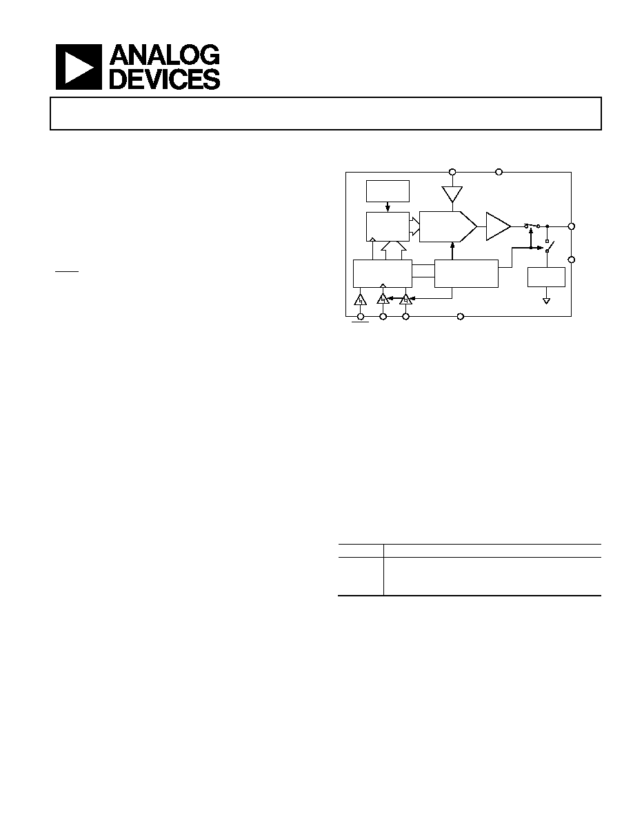
GENERAL DESCRIPTION
The AD5040 and the AD5060, members of the ADI nanoDAC
family, are low power, single 14-/16-bit buffered voltage-out
DACs that operate from a single 2.7 V to 5.5 V supply. The
AD5040/AD5060 parts offer a relative accuracy specification
of ±1 LSB and operation are guaranteed monotonic with a
±1 LSB DNL specification. The parts use a versatile 3-wire serial
interface that operates at clock rates up to 30 MHz and is
compatible with standard SPI®, QSPITM, MICROWIRETM, and
DSP interface standards. The reference for both the AD5040
and AD5060 is supplied from an external V
REF
pin. A reference
buffer is also provided on-chip. The AD5060 incorporates a
power-on reset circuit that ensures the DAC output powers up
to midscale or zero scale and remains there until a valid write
takes place to the device. The AD5040 and the AD5060 both
contain a power-down feature that reduces the current con-
sumption of the device to typically 330 nA at 5 V and provides
software-selectable output loads while in power-down mode.
The parts are put into power-down mode over the serial
interface. Total unadjusted error for the parts is <2 mV.
Both parts exhibit very low glitch on power-up.
FUNCTIONAL BLOCK DIAGRAM
AD5040/
AD5060
V
DD
V
OUT
V
REF
POWER-ON
RESET
DAC
REGISTER
DAC
INPUT
CONTROL
LOGIC
POWER-DOWN
CONTROL LOGIC
RESISTOR
NETWORK
REF(+)
SCLK
DIN
04767-
001
SYNC
DACGND
BUF
AGND
OUTPUT
BUFFER
Figure 1.
PRODUCT HIGHLIGHTS
1.
Available in a small, 8-lead SOT-23 package.
2.
14-/16-bit accurate, 1 LSB INL.
3.
Low glitch on power-up.
4.
High speed serial interface with clock speeds up to 30 MHz.
5.
Three power-down modes available to the user.
6.
Reset to known output voltage (midscale, zero scale).
Table 1. Related Devices
Part No.
Description
AD5061
2.7 V to 5.5 V, 16-bit nanoDAC D/A, 4 LSB INL, SOT-23
AD5062
2.7 V to 5.5 V, 16-bit nanoDAC D/A,1 LSB INL, SOT-23
AD5063
2.7 V to 5.5 V, 16-bit nanoDAC D/A, 1 LSB INL, MSOP

AD5040/AD5060
Rev. 0 | Page 2 of 24
TABLE OF CONTENTS
Features .............................................................................................. 1
Applications....................................................................................... 1
General Description ......................................................................... 1
Functional Block Diagram .............................................................. 1
Product Highlights ........................................................................... 1
Revision History ............................................................................... 2
Specifications..................................................................................... 3
Timing Characteristics..................................................................... 5
Absolute Maximum Ratings............................................................ 6
ESD Caution.................................................................................. 6
Pin Configuration and Function Descriptions............................. 7
Typical Performance Characteristics ............................................. 8
Terminology .................................................................................... 14
Theory of Operation ...................................................................... 15
DAC Architecture....................................................................... 15
Reference Buffer ......................................................................... 15
Serial Interface ............................................................................ 15
Power-On reset ........................................................................... 16
Software Reset............................................................................. 16
Power-Down Modes .................................................................. 17
Microprocessor Interfacing....................................................... 17
Applications..................................................................................... 19
Choosing a Reference for the AD5040/ AD5060................... 19
Bipolar Operation Using the AD5040/ AD5060.................... 19
Using the AD5040/AD5060 with a Galvanically Isolated
Interface Chip ............................................................................. 20
Power Supply Bypassing and Grounding................................ 20
Outline Dimensions ....................................................................... 21
Ordering Guide .......................................................................... 21
REVISION HISTORY
10/05--Revision 0: Initial Version

AD5040/AD5060
Rev. 0 | Page 3 of 24
SPECIFICATIONS
V
DD
= 5.5 V, V
REF
= 4.096 V @ R
L
= unloaded, C
L
= unloaded; T
MIN
to T
MAX
, unless otherwise noted.
Table 2.
A, B Grade
1
Parameter Min
Typ
Max
Unit
Test
Conditions/Comments
STATIC PERFORMANCE
Resolution 16
Bits
AD5060
14
Bits
AD5040
Relative Accuracy (INL)
2
±0.5
±1
LSB
-40°C to +85°C, AD5040/AD5060
±0.5
±1.5
-40°C to +125°C, AD5060 Y grade
Total Unadjusted Error (TUE)
2
±0.1
±2.0
mV
-40°C to +85°C, AD5040/AD5060
±0.1
±2.0
-40°C to +125°C, AD5060 Y grade
Differential Nonlinearity (DNL)
2
±0.5 ±1 LSB
Guaranteed monotonic,
-40°C to +85°C, AD5040/AD5060
±0.5
±1
Guaranteed monotonic,
-40°C to +125°C, Y grade
Gain Error
±0.01
±0.02
% of FSR
T
A
= -40°C to +85°C, AD5040/AD5060
±0.01
±0.03
T
A
= -40°C to +125°C AD5060 Y grade
Gain Error Temperature Coefficient
1
ppm of FSR/°C
Offset Error
±0.02
±1.5
mV
T
A
= -40°C to + 85°C, AD5040/AD5060
±0.02
±2.0
T
A
= -40°C to + 125°C, AD5060 Y grade
Offset Error Temperature Coefficient
0.5
V/°C
Full-Scale Error
±0.05
±2.0
mV
All 1s loaded to DAC register,
AD5040 AD5060; T
A
= -40°C to +85°C
±0.05
±2.0
All 1s loaded to DAC register,
T
A
= -40°C to +125°C, AD5060 Y grade
OUTPUT CHARACTERISTICS
3
Output Voltage Range
0
V
REF
V
Output Voltage Settling Time
4
s
¼ scale to ¾ scale code transition to
±1 LSB, R
L
= 5 k
Output Noise Spectral Density
64
nV/
Hz
DAC code = midscale, 1 kHz
Output Voltage Noise
6
V p-p
DAC code = midscale , 0.1 Hz to 10 Hz
bandwidth
Digital-to-Analog Glitch Impulse
2
nV-s
1 LSB change around code 57386,
R
L
= 5 k, C
L
= 200 pF
Digital Feedthrough
0. 003
nV-s
DAC code = full scale
DC Output Impedance (Normal)
0. 015
Output impedance tolerance ±10%
DC Output Impedance (Power-Down)
(Output Connected to 1 k
Network)
4
1
k
Output impedance tolerance ±400
(Output Connected to 100 k
Network)
100
k
Output impedance tolerance ±20 k
Capacitive Load Stability
1
nF
Loads used R
L
= 5 k, R
L
= 100 k, R
L
=
Slew Rate
1. 2
V/s
¼ scale to ¾ scale code transition to
±1 LSB, R
L
= 5 k, C
L
= 200 pF
Short-Circuit Current
60
ma
DAC code = full scale, output shorted to
GND, T
A
= 25°C
45
DAC code = zero scale, output shorted to
V
DD
, T
A
= 25°C
DAC Power-Up Time
4.5
s
Time to exit power-down mode to normal
mode of AD5060, 24
th
clock edge to 90%
of DAC final value, output unloaded
DC Power Supply Rejection Ratio
-92.11
db
V
DD
± 10%, DAC code = full scale
Wideband Spurious-Free Dynamic
-67
db
Output frequency = 10 kHz

AD5040/AD5060
Rev. 0 | Page 4 of 24
A, B Grade
1
Parameter Min
Typ
Max
Unit
Test
Conditions/Comments
Range (SFDR)
REFERENCE INPUT/OUTPUT
V
REF
Input Range
5
2
V
DD
- 50
mV
Input Current (Power-Down)
±0.1
A
Zero scale loaded
Input Current (Normal)
±0.5
A
DC Input Impedance
1
M
LOGIC INPUTS
Input Current
6
±1 ±2 A
V
IL
, Input Low Voltage
0.8
V
V
DD
= 4.5 V to 5.5 V
0.8
V
DD
= 2.7 V to 3.6 V
V
IH
, Input High Voltage
2.0
V
V
DD
= 2.7 V to 5.5 V
1.8
V
DD
= 2.7 V to 3.6 V
Pin Capacitance
4
pF
POWER REQUIREMENTS
V
DD
2.7
5.5
V
All digital inputs at 0 V or V
DD
I
DD
(Normal Mode)
DAC active and excluding load current
V
DD
= 2.7 V to 5.5 V
1.0
0. 82
1.2
1. 0
mA
V
IN
= V
DD
and V
IL
= GND, V
DD
= 5.0 V,
V
REF
= 4.096 V, code = midscale
V
IN
= V
DD
and V
IL
= GND, V
DD
= 3.0 V,
V
REF
= 2.7 V, code = midscale
I
DD
(All Power-Down Modes)
V
DD
= 2.5 V to 5.5 V
0.33
1
A
V
IH
= V
DD
and V
IL
= GND, V
DD
= 5.5 V,
V
REF
= 4.096 V, code = midscale
0.065
V
IH
= V
DD
and V
IL
= GND, V
DD
= 3.0 V,
V
REF
= 4.096 V, code = midscale
1
Temperature range for the B grade is -40°C to + 85° C, typical at 25°C; temperature range for the Y grade is -40°C to +125°C.
2
Linearity calculated using a reduced code range (160 to code 65535 for AD5060 ) and (40 to code 16383 for AD5040).
3
Guaranteed by design and characterization, not production tested.
4
1 k power-down network not available with the AD5040.
5
The typical output supply headroom performance for various reference voltages at -40°C can be seen in Figure 26.
6
Total current flowing into all pins.
AD5040/AD5060
Rev. 0 | Page 5 of 24
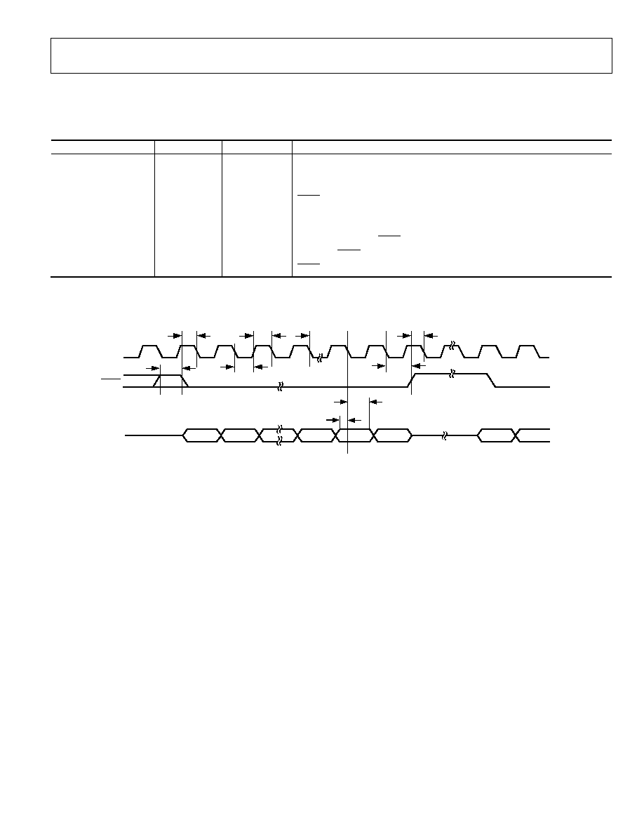
TIMING CHARACTERISTICS
V
DD
= 2.7 V to 5.5 V; all specifications T
MIN
to T
MAX
, unless otherwise noted.
Table 3.
Parameter Limit
1
Unit Test
Conditions/Comments
t
1
2
33
ns min
SCLK cycle time
t
2
5
ns min
SCLK high time
t
3
3
ns min
SCLK low time
t
4
10 ns
min
SYNC to SCLK falling edge setup time
t
5
3
ns min
Data setup time
t
6
2
ns min
Data hold time
t
7
0 ns
min
SCLK falling edge to SYNC rising edge
t
8
12 ns
min
Minimum SYNC high time
t
9
9 ns
min
SYNC rising edge to next SCLK fall ignore
1
All input signals are specified with tr = tf = 1 ns/V (10% to 90% of V
DD
) and timed from a voltage level of (V
IL
+ V
IH
)/2.
2
Maximum SCLK frequency is 30 MHz.
t
4
t
3
t
2
t
5
t
7
t
6
D0
D1
D2
D22
D23
SYNC
SCLK
04767-002
t
9
t
1
t
8
D23
D22
DIN
Figure 2. AD5060 Timing Diagram
AD5040/AD5060
Rev. 0 | Page 6 of 24
ABSOLUTE MAXIMUM RATINGS
Table 4.
Parameter Rating
V
DD
to GND
-0.3 V to +7.0 V
Digital Input Voltage to GND
-0.3 V to V
DD
+ 0.3 V
V
OUT
to GND
-0.3 V to V
DD
+ 0.3 V
V
REF
to GND
-0.3 V to V
DD
+ 0.3 V
Operating Temperature Range
Industrial (A, B Grade)
-40°C to +85°C
Extended Automotive Temperature
Range (Y Grade)
-40°C to +125°C
Storage Temperature Range
-65°C to +150°C
Maximum Junction Temperature
150°C
SOT-23 Package
Power Dissipation
(T
J
max - T
A
)/
JA
JA
Thermal Impedance
206°C/W
Jc
Thermal Impedance
91°C/W
Reflow Soldering (Pb-free)
Peak Temperature
260°C
Time-at-Peak Temperature
10 sec to 40 sec
ESD (AD5040/AD5060)
1. 5 kV
Stresses above those listed under Absolute Maximum Ratings
may cause permanent damage to the device. This is a stress
rating only; functional operation of the device at these or any
other conditions above those indicated in the operational
section of this specification is not implied. Exposure to absolute
maximum rating conditions for extended periods may affect
device reliability.
This device is a high performance integrated circuit with an
ESD rating of <2 kV. It is ESD sensitive. Proper precautions
should be taken for handling and assembly.
ESD CAUTION
ESD (electrostatic discharge) sensitive device. Electrostatic charges as high as 4000 V readily accumulate on
the human body and test equipment and can discharge without detection. Although this product features
proprietary ESD protection circuitry, permanent damage may occur on devices subjected to high energy
electrostatic discharges. Therefore, proper ESD precautions are recommended to avoid performance
degradation or loss of functionality.
AD5040/AD5060
Rev. 0 | Page 7 of 24
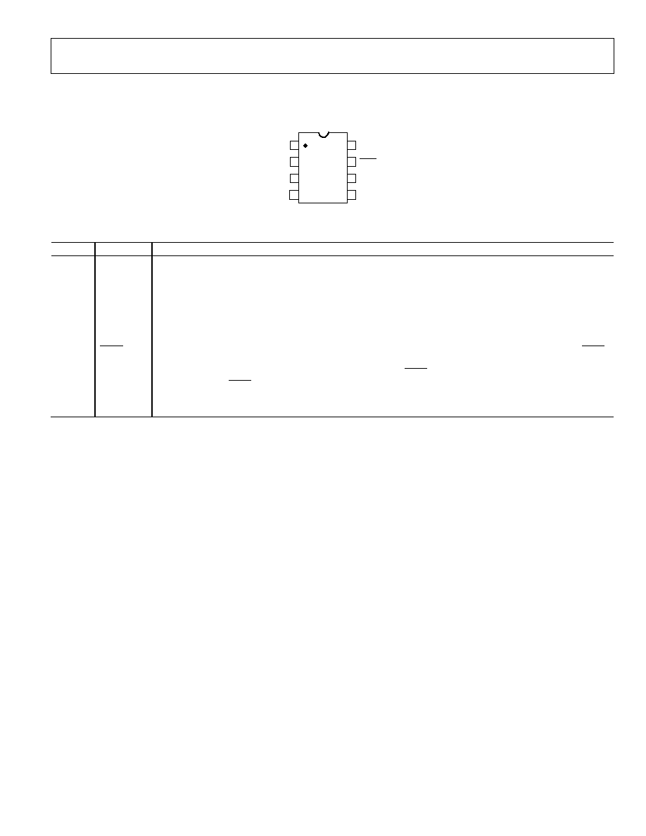
PIN CONFIGURATION AND FUNCTION DESCRIPTIONS
AD5040/
AD5060
TOP VIEW
(Not to Scale)
V
OUT
SYNC
1
8
AGND
SCLK
2
7
DIN
DACGND
3
6
04767-003
V
REF
4
5
V
DD
Figure 3. Pin Configuration
Table 5. Pin Function Descriptions
Pin No.
Mnemonic
Description
1 DIN Serial Data Input. These parts have a 16-/24-bit shift register. Data is clocked into the register on the falling edge of
the serial clock input.
2
V
DD
Power Supply Input. These parts can be operated from 2.7 V to 5.5 V and V
DD
should be decoupled to GND.
3 V
REF
Reference Voltage Input.
4 V
OUT
Analog Output Voltage from DAC.
5
AGND
Ground Reference Point for Analog Circuitry.
6
DACGND
Ground Input to the DAC Core.
7
SYNC
Level-Triggered Control Input (Active Low). This is the frame synchronization signal for the input data. When SYNC
goes low, it enables the input shift register and data is transferred in on the falling edges of the following clocks.
The DAC is updated following the 16th/24th clock cycle unless SYNC is taken high before this edge, in which case
the rising edge of SYNC acts as an interrupt, and the write sequence is ignored by the DAC.
8 SCLK Serial Clock Input. Data is clocked into the input shift register on the falling edge of the serial clock input. Data can
be transferred at rates up to 30 MHz.
AD5040/AD5060
Rev. 0 | Page 8 of 24
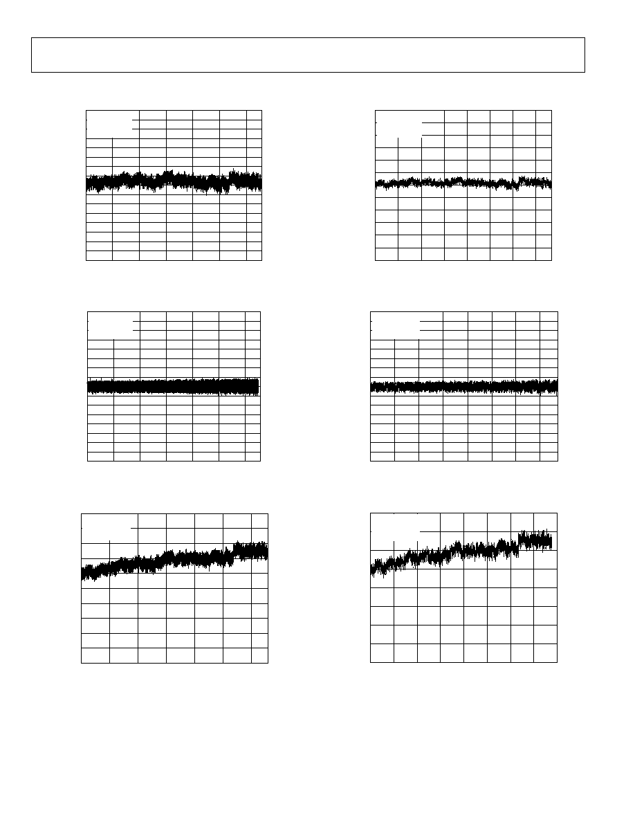
TYPICAL PERFORMANCE CHARACTERISTICS
1.6
1.6
1.4
1.2
1.0
0.8
0.6
0.4
0.2
0
0.2
0.4
0.6
0.8
1.0
1.2
1.4
160
10160
30160
50160
60160
20160
40160
04767-040
I
N
L E
RROR (LS
B
)
DAC CODE
V
DD
= 5.5V
V
REF
= 4.096V
T
A
= 25
°
C
Figure 4. Typical AD5060 INL Plot
1.6
1.6
1.4
1.2
1.0
0.8
0.6
0.4
0.2
0
0.2
0.4
0.6
0.8
1.0
1.2
1.4
160
10160
30160
50160
60160
20160
40160
04767-039
DNL E
R
ROR (LS
B
)
DAC CODE
V
DD
= 5.5V
V
REF
= 4.096V
T
A
= 25
°
C
Figure 5. Typical AD5060 DNL Plot
0.10
0.10
0.08
0.06
0.04
0.02
0
0.02
0.04
0.06
0.08
160
10160
30160
50160
60160
20160
40160
04767-041
TUE
E
RROR (mV
)
DAC CODE
V
DD
= 5.5V
V
REF
= 4.096V
T
A
= 25
°
C
Figure 6. Typical AD5060 TUE Plot
0.6
0.6
0.5
0.4
0.3
0.2
0.1
0.1
0
0.2
0.3
0.4
0.5
160
2260
8560
12760 14860
4360
6460
10660
04767-061
I
N
L E
RROR (LS
B
)
DAC CODE
V
DD
= 5.5V
V
REF
= 4.096V
T
A
= 25
°
C
Figure 7. Typical AD5040 INL Plot
0.40
0.40
0.35
0.30
0.25
0.20
0.15
0.10
0.05
0
0.05
0.10
0.15
0.20
0.25
0.30
0.35
160
2260
6460
10660
12760
14860
4360
8560
04767-060
DNL E
RROR (LS
B
)
DAC CODE
V
DD
= 5.5V
V
REF
= 4.096V
T
A
= 25
°
C
Figure 8. Typical AD5040 DNL Plot
0.020
0.020
0.015
0.010
0.005
0
0.005
0.010
0.015
160
2260
8560
12760 14860 16960
4360
6460
10660
04767-062
TUE
E
RROR (mV
)
DAC CODE
V
DD
= 5.5V
V
REF
= 4.096V
T
A
= 25
°
C
Figure 9. Typical AD5040 TUE Plot
AD5040/AD5060
Rev. 0 | Page 9 of 24
04767-009
2.0
1.6
1.4
1.2
1.0
0.8
0.6
0.4
0.2
0
0.2
0.4
0.6
0.8
1.0
1.2
1.4
1.6
5.5
5.0
4.5
4.0
3.5
3.0
2.5
INL E
RROR (LS
B
)
REFERENCE VOLTAGE (V)
MAX INL ERROR @ V
DD
= 5.5V
MIN INL ERROR @ V
DD
= 5.5V
T
A
= 25
°
C
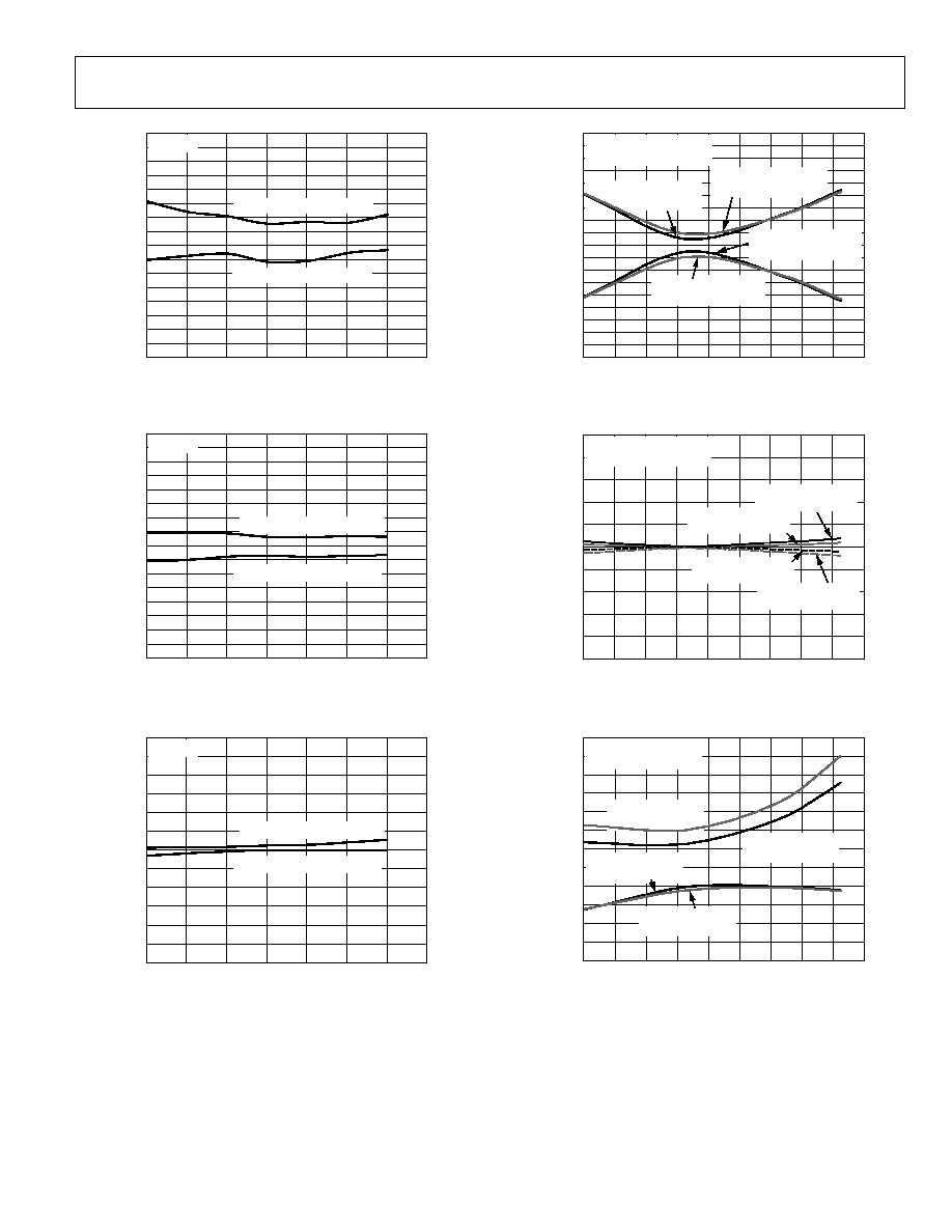
Figure 10. INL vs. Reference Input Voltage
1
04767-010
2.0
1.6
1.4
1.2
1.0
0.8
0.6
0.4
0.2
0
0.2
0.4
0.6
0.8
1.0
1.2
1.4
1.6
5.5
5.0
4.5
4.0
3.5
3.0
2.5
DNL E
RROR (LS
B
)
REFERENCE VOLTAGE (V)
MAX DNL ERROR @ V
DD
= 5.5V
MIN DNL ERROR @ V
DD
= 5.5V
T
A
= 25
°
C
Figure 11. DNL vs. Reference Input Voltage
1
04767-011
2.0
1.2
1.0
0.8
0.6
0.4
0.2
0
0.2
0.4
0.6
0.8
1.0
1.2
5.5
5.0
4.5
4.0
3.5
3.0
2.5
TUE
E
RROR (mV
)
REFERENCE VOLTAGE (V)
MAX TUE ERROR @ V
DD
= 5.5V
MIN TUE ERROR @ V
DD
= 5.5V
T
A
= 25
°
C
Figure 12. TUE vs. Reference Input Voltage
1
1.8
1.8
1.6
1.4
1.2
1.0
0.8
0.6
0.4
0.2
0
0.2
0.4
0.6
0.8
1.0
1.2
1.4
1.6
40
140
120
100
80
60
40
20
0
20
04767-067
OFFSET ER
R
O
R
(
m
V)
TEMPERATURE (°C)
MAX OFFSET ERROR @
V
DD
= 5.5V
MAX OFFSET ERROR @
V
DD
= 2.7V
MIN OFFSET ERROR @
V
DD
= 2.7V
V
DD
= 5.5V, V
REF
= 4.096V
V
DD
= 2.7V, V
REF
= 2.0V
MIN OFFSET ERROR @
V
DD
= 5.5V
Figure 13. Typical Offset Error vs. Temperature
1
0.5
0.5
0.4
0.3
0.2
0.1
0
0.1
0.2
0.3
0.4
40
140
120
100
80
60
40
20
0
20
04767-066
GAIN E
RROR (% FS
R)
TEMPERATURE (°C)
V
DD
= 5.5V, V
REF
= 4.096V
V
DD
= 2.7V, V
REF
= 2.0V
MAX GAIN ERROR @
V
DD
= 5.5V
MAX GAIN ERROR @
V
DD
= 2.7V
MIN GAIN ERROR @
V
DD
= 5.5V
MIN GAIN ERROR @
V
DD
= 2.7V
Figure 14. Typical Gain Error vs. Temperature
1
1.4
1.0
0.8
0.6
0.4
0.2
0
0.2
0.4
0.6
0.8
1.0
1.2
40
140
120
100
80
60
40
20
0
20
04767-069
INL E
RROR (LS
B
)
TEMPERATURE (°C)
V
DD
= 5.5V, V
REF
= 4.096V
V
DD
= 2.7V, V
REF
= 2.0V
MAX INL ERROR @
V
DD
= 5.5V
MAX INL ERROR @
V
DD
= 2.7V
MIN INL ERROR @
V
DD
= 2.7V
MIN INL ERROR @
V
DD
= 5.5V
Figure 15. Typical INL Error vs. Temperature
1
1
AD5060 only.
AD5040/AD5060
Rev. 0 | Page 10 of 24
1.0
1.0
0.8
0.6
0.4
0.2
0
0.2
0.4
0.6
0.8
40
140
120
100
80
60
40
20
0
20
04767-071
DNL E
RROR (LS
B
)
TEMPERATURE (°C)
V
DD
= 5.5V, V
REF
= 4.096V
V
DD
= 2.7V, V
REF
= 2.0V
MAX DNL ERROR @
V
DD
= 5.5V
MAX DNL ERROR @
V
DD
= 2.7V
MIN DNL ERROR @
V
DD
= 2.7V
MIN DNL ERROR @
V
DD
= 5.5V
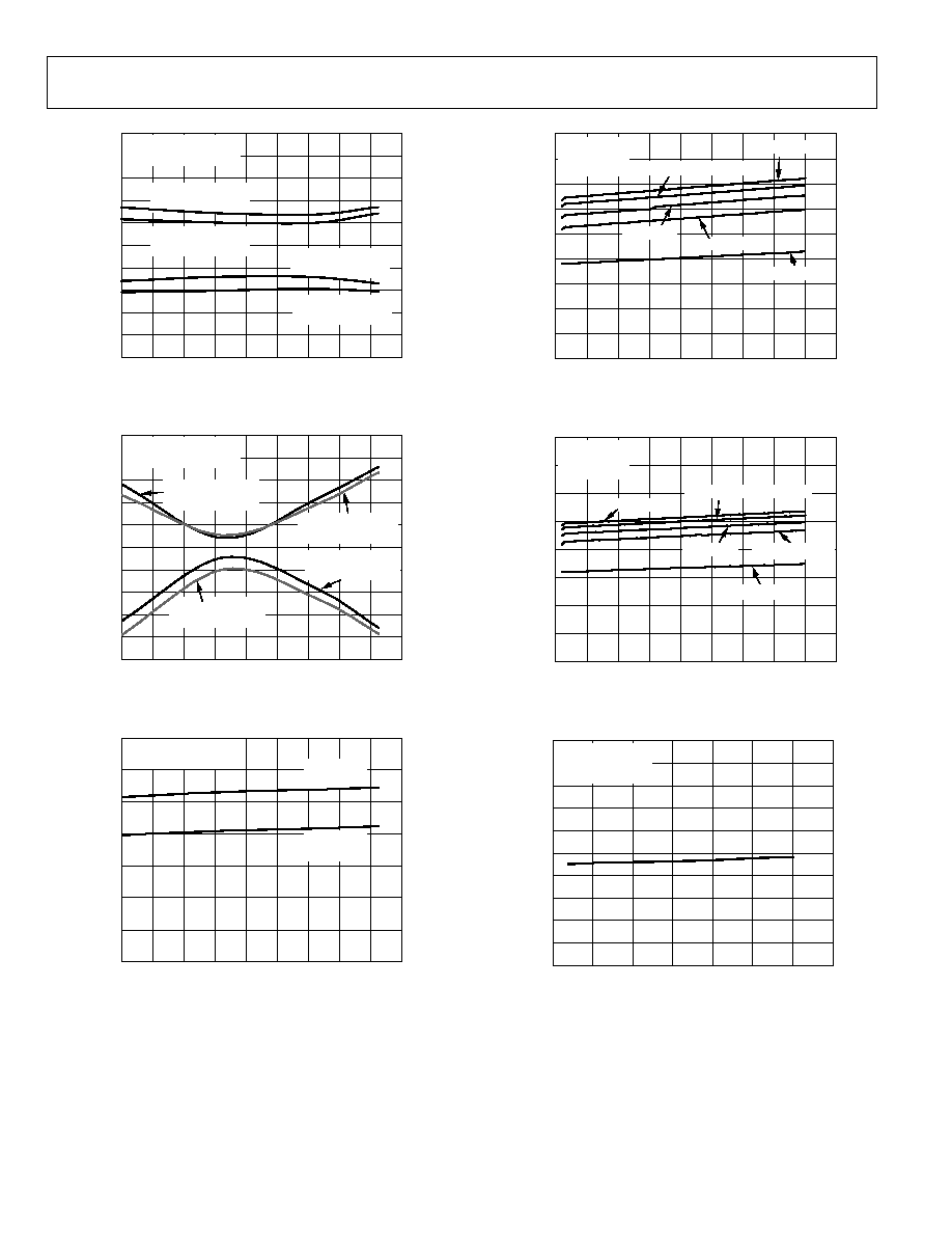
Figure 16. Typical DNL Error vs. Temperature
1
MAX TUE ERROR @
V
DD
= 5.5V
MAX TUE ERROR @
V
DD
= 2.7V
MIN TUE ERROR @
V
DD
= 2.7V
MIN TUE ERROR @
V
DD
= 5.5V
1.0
1.0
0.8
0.6
0.4
0.2
0
0.2
0.4
0.6
0.8
40
140
120
100
80
60
40
20
0
20
04767-068
TUE
E
RROR (mV
)
TEMPERATURE (°C)
V
DD
= 5.5V, V
REF
= 4.096V
V
DD
= 2.7V, V
REF
= 2.0V
Figure 17. Typical TUE Error vs. Temperature
1
1.4
0
0.2
0.4
0.6
0.8
1.0
1.2
40
140
120
100
80
60
40
20
0
20
04767-072
I
DD
(mA)
TEMPERATURE (°C)
V
DD
= 5.5V, V
REF
= 4.096V
V
DD
= 2.7V, V
REF
= 2.0V
MAX I
DD
@
V
DD
= 5.5V
MAX I
DD
@
V
DD
= 2.7V
Figure 18. Typical Supply Current vs. Temperature
1
1.8
1.6
1.4
1.2
1.0
0.8
0.6
0.4
0.2
0
0
5M
10M
15M
20M
25M
30M
35M
40M
45M
04767-044
I
DD
(mA)
FREQUENCY (Hz)
V
DD
= 5.5V
V
REF
= 4.096V
T
A
= 25
°
C
FULL-SCALE
THREE QUARTER SCALE
QUARTER-SCALE
MID-SCALE
ZERO-SCALE
Figure 19. Typical Supply Current vs. Frequency @ 5.5 V
1
1.4
1.2
1.0
0.8
0.6
0.4
0.2
0
0
5M
10M
15M
20M
25M
30M
35M
40M
45M
04767-045
I
DD
(mA)
V
DD
= 3V
V
REF
= 2.5V
T
A
= 25
°
C
1.6
FREQUENCY (Hz)
FULL-SCALE
THREE QUARTER SCALE
QUARTER-SCALE
MID-SCALE
ZERO-SCALE
Figure 20. Typical Supply Current vs. Frequency @ 3 V
1
04767-015
2.5
0
2.0
1.8
1.6
1.4
1.2
1.0
0.8
0.6
0.4
0.2
6.0
5.5
5.0
4.5
4.0
3.5
3.0
I
DD
(
A)
SUPPLY VOLTAGE (V)
V
REF
= 2.5V
T
A
= 25
°
C
CODE = MIDSCALE
Figure 21. Typical Supply Current vs. Supply Voltage
1
1
AD5060 only.
AD5040/AD5060
Rev. 0 | Page 11 of 24
04767-014
0
0
3.00
2.75
2.50
2.25
2.00
1.75
1.50
1.25
1.00
0.75
0.50
0.25
70000
60000
50000
40000
30000
20000
10000
I
DD
(mA)
DAC CODE
V
DD
= 3.0V, V
REF
= 2.5V
V
DD
= 5.5V, V
REF
= 4.096V
T
A
= 25
°
C
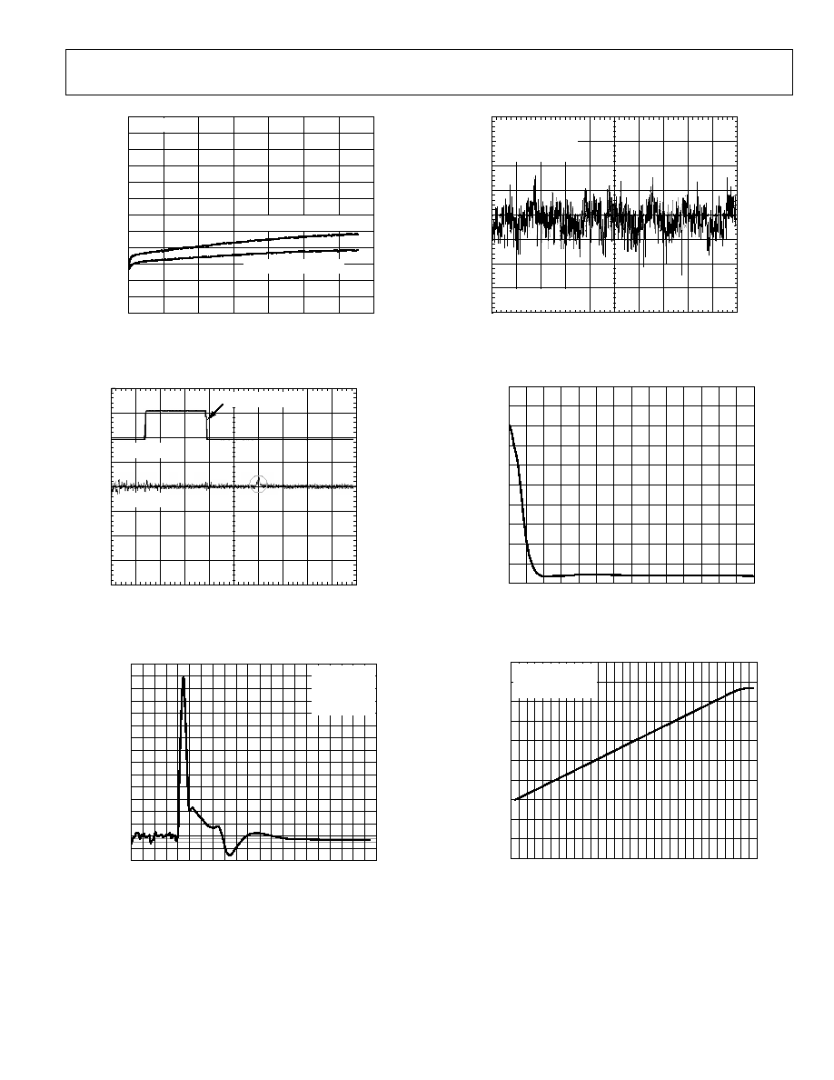
Figure 22. Typical Supply Current vs. Digital Input Code
1
04767-017
CH2 50mV/DIV
CH1 2V/DIV
TIME BASE 400ns/DIV
24TH CLOCK FALLING
CH1 = SCLK
CH2 = V
OUT
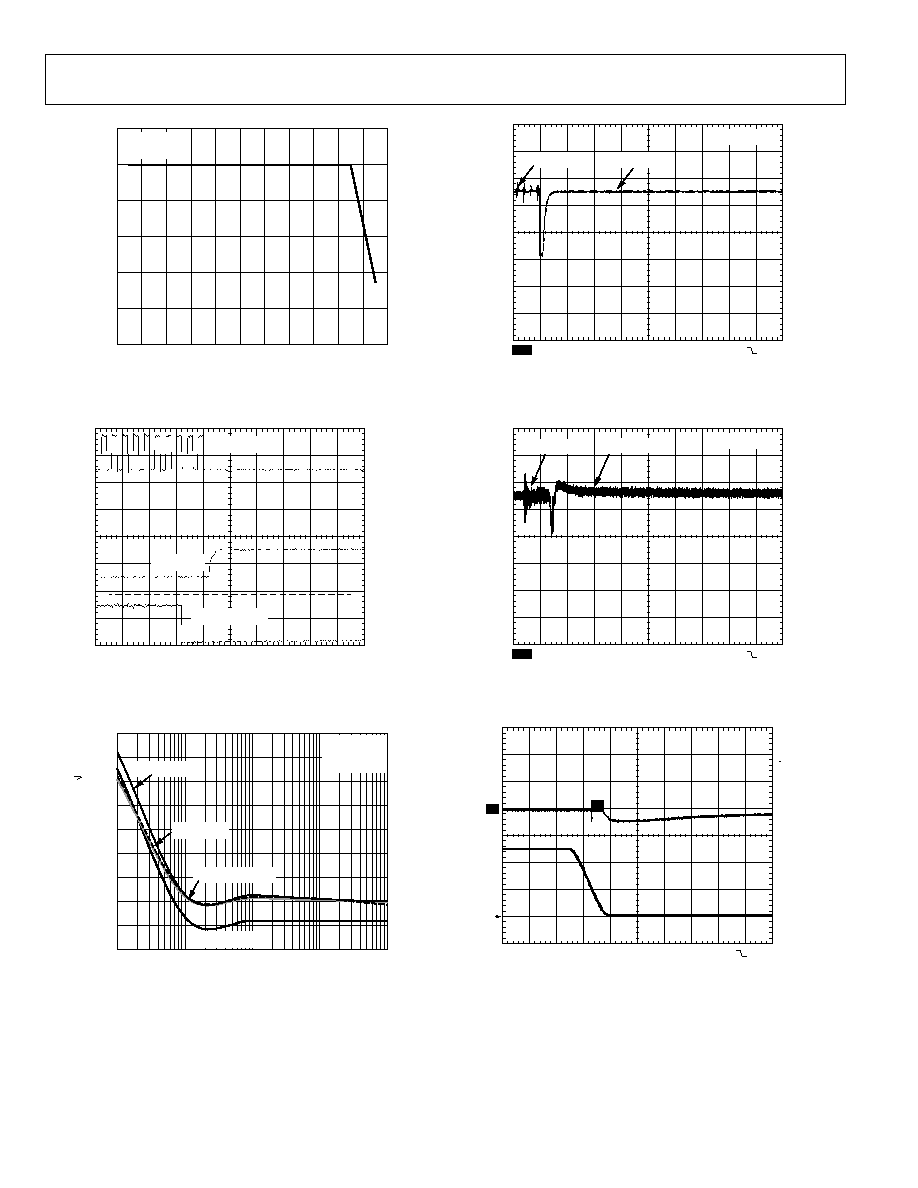
Figure 23. AD5060 Digital-to-Analog Glitch Impulse
(See Figure 24)
0.117
0.101
0.102
0.103
0.104
0.105
0.106
0.107
0.108
0.109
0.111
0.110
0.112
0.113
0.114
0.115
0.116
0
25
50
75
100
125
150
175
200
225
250
275
300
325
350
375
400
425
450
475
500
525
04767-043
AMP
L
ITUDE
SAMPLES
V
DD
= 5V
V
REF
= 4.096V
R = 5k
C = 220pF
CODE = 57386
Figure 24. AD5060 Digital-to-Analog Glitch Energy
1
AD5060 only.
04767-020
V
DD
= 3V
DAC = FULL SCALE
V
REF
= 2.7V
T
A
= 25°C
Y AXIS = 2
V/DIV
X AXIS = 4s/DIV
Figure 25. 0.1 Hz to 10 Hz Noise Plot
04767-091
2.7 2.9 3.1 3.3 3.5 3.7 3.9 4.1 4.3 4.5 4.7 4.9 5.1
0
0.50
0.45
0.40
0.35
0.30
0.25
0.20
0.15
0.10
0.05
5.5
5.3
HE
ADROOM (V
)
REFERENCE VOLTAGE (V)
Figure 26. V
DD
Headroom vs. Reference Voltage
5.05
5.00
4.95
4.90
4.85
4.80
4.75
4.70
4.65
4.60
4.55
4.70 4.72 4.74 4.76 4.78 4.80 4.82 4.84 4.86 4.88 4.90 4.92 4.94 4.96 4.98 5.00
04767-042
DAC OUTP
UT V
O
LTAGE
(V
)
V
REF
(V)
V
DD
= 5.0V
T
A
= 25
°
C
DAC = FULL-SCALE
Figure 27. Output Voltage vs. Reference Voltage
AD5040/AD5060
Rev. 0 | Page 12 of 24
5.005
4.975
4.980
4.985
4.990
4.995
5.000
5.50
5.00
5.05
5.10
5.15
5.20
5.25
5.30
5.35
5.40
5.45
04767-065
DAC OUTP
UT (V
)
V
DD
(V)
V
REF
= 5V
T
A
= 25°C
Figure 28. Typical Output vs. Supply Voltage
04767
-019
CH2 2V/DIV
CH1 2V/DIV
TIME BASE = 5.00
s
CH3 2V
CH3 = SCLK
CH2 = V
OUT
CH1 = TRIGGER
Figure 29. Time to Exit Power-Down to Midscale
50
100
1k
10k
100k
1M
04767-046
N
OISE SPEC
TR
A
L
D
E
N
S
ITY (
n
V/ H
z
)
V
DD
= 5V
V
REF
= 4.096V
T
A
= 25
°
C
400
350
300
250
200
150
100
50
0
FREQUENCY (Hz)
QUARTER-SCALE
ZERO-SCALE
FULL-SCALE
MID-SCALE
Figure 30. Noise Spectral Density
04767-047
CH4
50.0mV
M4.00
s
CH1 1.64V
C4 = 143mV p-p
1k
TO GND
ZERO-SCALE
Figure 31. Glitch upon Entering Software Power-Down to Zero Scale
04767-048
CH4
20.0mV
M1.00
s
CH1 1.64V
C4 = 50mV p-p
1k
TO GND
ZERO-SCALE
Figure 32. Glitch upon Exiting Software Power-Down to Zero Scale
04767-049
CH3 2.00V
CH2 50mV
M1.00ms
CH3 1.36V
2
C2
25mV p-p
C3
4.96V p-p
C3 FALL
935.0
s
C3 RISE
s
NO VALID
EDGE
3
T
T
Figure 33. Glitch upon Entering Hardware Power-Down to Three-State
AD5040/AD5060
Rev. 0 | Page 13 of 24
04767-050
CH3 2.00V
CH2 50mV
M1.00ms
CH3 1.36V
2
C2
30mV p-p
C3
4.96V p-p
C3 FALL
s
NO VALID
EDGE
C3 RISE
946.2
s
3
T
T
2.1
1.0
1.1
1.2
1.3
1.4
1.5
1.6
1.7
1.8
1.9
2.0
10
s
9.96
s
8
s
6
s
4
s
2
s
0
2
s
4
s
6
s
8
s
04767-052
V
DD
= 5.5V
V
REF
= 4.096V
10% TO 90% RISE TIME = 0.688
s
SLEW RATE = 1.16V/
s
DAC
OUTPUT
1.04V
2.04V
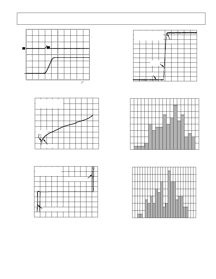
Figure 34. Glitch upon Exiting Hardware Power-Down to Zero Scale
Figure 37. Typical Output Slew Rate
0.0010
0.0008
0.0006
0.0004
0.0002
0
0.0002
0.0004
0.0006
0.0008
25 20 15 10
5
0
5
10
15
20
25
30
04767-051
VOLTAGE (V)
CURRENT (mA)
CODE = MID-SCALE
V
DD
= 5V, V
REF
= 4.096V
V
DD
= 3V, V
REF
= 2.5V
V
DD
= 5.5V
V
DD
= 3V
16
14
0
2
4
6
8
10
12
0.83
MORE
0.91
0.90
0.89
0.88
0.87
0.86
0.85
0.84
04767-075
FRE
Q
UE
NCY
BIN
Figure 35. Typical Output Load Regulation
Figure 38. I
DD
Histogram V
DD
= 3.0 V
0.10
0.10
0.08
0.06
0.04
0.02
0
0.02
0.04
0.06
0.08
25 20 15 10
5
0
5
10
15
20
25
30
04767-063
V
OUT
(V
)
I
OUT
(mA)
CODE = MIDSCALE
V
DD
= 5V, V
REF
= 4.096V
V
DD
= 3V, V
REF
= 2.5V
V
DD
= 3V, V
REF
= 2.5V
V
DD
= 5V, V
REF
= 4.096V
14
0
2
4
6
8
10
12
1.00 1.01 1.02 1.03 1.04 1.05 1.06 1.07 1.08 1.09 1.10 1.11MORE
04767-076
FRE
Q
UE
NCY
BIN
Figure 36. Typical Current Limiting Plot
Figure 39. I
DD
Histogram V
DD
= 5.0 V

AD5040/AD5060
Rev. 0 | Page 14 of 24
TERMINOLOGY
Relative Accuracy
For the DAC, relative accuracy or integral nonlinearity (INL) is
a measure of the maximum deviation, in LSBs, from a straight
line passing through the endpoints of the DAC transfer
function. A typical AD5060 INL vs. code plot is shown in
Figure 4.
Differential Nonlinearity (DNL)
Differential nonlinearity is the difference between the measured
change and the ideal 1 LSB change between any two adjacent
codes. A specified differential nonlinearity of ±1 LSB maximum
ensures monotonicity. This DAC is guaranteed monotonic by
design. A typical AD5060 DNL vs. code plot is shown in Figure 5.
Offset Error
Offset error is a measure of the output error when zero code
(0x0000) is loaded to the DAC register. Ideally, the output
should be 0 V. The zero-code error is always positive in the
AD5040/AD5060 because the output of the DAC cannot go
below 0 V. This is due to a combination of the offset errors in
the DAC and output amplifier. Zero-code error is expressed
in mV.
Full-Scale Error
Full-scale error is a measure of the output error when full-scale
code (0xFFFF AD5060, 0x3FFF AD5040) is loaded to the DAC
register. Ideally, the output should be V
DD
- 1 LSB. Full-scale
error is expressed in percent of full-scale range.
Gain Error
This is a measure of the span error of the DAC. It is the devia-
tion in slope of the DAC transfer characteristic from ideal,
expressed as a percent of the full-scale range.
Total Unadjusted Error (TUE)
Total unadjusted error is a measure of the output error taking
all the various errors into account. A typical AD5060 TUE vs.
code plot is shown in Figure 6.
Offset Error Drift
This is a measure of the change in zero-code error with a
change in temperature. It is expressed in V/°C.
Gain Error Drift
This is a measure of the change in gain error with changes in
temperature. It is expressed in (ppm of full-scale range)/°C.
Digital-to-Analog Glitch Impulse
Digital-to-analog glitch impulse is the impulse injected into the
analog output when the input code in the DAC register changes
state. It is normally specified as the area of the glitch in nV-s
and is measured when the digital input code is changed by
1 LSB at the worst case code 53786; see Figure 23 and Figure 24.
The expanded view in Figure 23 shows the glitch generated
following completion of the calibration routine; Figure 24
zooms in on this glitch.
Digital Feedthrough
Digital feedthrough is a measure of the impulse injected into
the analog output of the DAC from the digital inputs of the
DAC, but is measured when the DAC output is not updated. It
is specified in nV-s and measured with a full-scale code change
on the data bus--that is, from all 0s to all 1s, and vice versa.
AD5040/AD5060
Rev. 0 | Page 15 of 24
THEORY OF OPERATION
The AD5040/AD5060 are single 14-/16-bit, serial input, voltage
output DACs. The parts operate from supply voltages of 2.7 V
to 5.5 V. Data is written to the AD5060 in a 24-bit word format,
and to the AD5040 in a 16-bit word format, via a 3-wire serial
interface.
Both the AD5040 and AD5060 incorporate a power-on reset
circuit that ensures the DAC output powers up to a known out-
put state (midscale or zero-scale, see the Ordering Guide). The
devices also have a software power-down mode that reduces the
typical current consumption to less than 1 a.
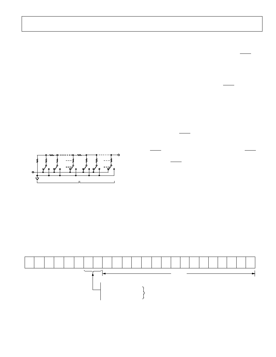
DAC ARCHITECTURE
The DAC architecture of the AD5060 consists of two matched
DAC sections. A simplified circuit diagram is shown in
Figure 40. The 4 MSBs of the 16-bit data-word are decoded to
drive 15 switches, E1 to E15. Each of these switches connects
1 of 15 matched resistors to either DACGND or the V
REF
buffer
output.
The remaining 12 bits of the data-word drive switches
S0 to S11 of a 12-bit voltage mode R-2R ladder network.
2R
04767-
027
S0
V
REF
2R
S1
2R
S11
2R
E1
2R
E2
2R
E15
2R
V
OUT
12-BIT R-2R LADDER
FOUR MSBs DECODED INTO
15 EQUAL SEGMENTS
Figure 40. AD5060 DAC Ladder Structure
REFERENCE BUFFER
The AD5040 andAD5060 operate with an external reference.
The reference input (V
REF
) has an input range of 2 V to
V
DD
- 50 mV. This input voltage is then used to provide a
buffered reference for the DAC core.
SERIAL INTERFACE
The AD5060/AD5040 have a 3-wire serial interface (SYNC,
SCLK, and DIN), which is compatible with SPI, QSPI, and
MICROWIRE interface standards, as well as most DSPs.
Figure 2 shows a timing diagram of a typical AD5060 write
sequence.
The write sequence begins by bringing the SYNC line low. For
the AD5060, data from the DIN line is clocked into the 24-bit
shift register on the falling edge of SCLK. The serial clock
frequency can be as high as 30 MHz, making these parts
compatible with high speed DSPs. On the 24th falling clock
edge, the last data bit is clocked in and the programmed
function is executed (that is, a change in the DAC output or a
change in the mode of operation).
At this stage, the SYNC line can be kept low or be brought
high. In either case, it must be brought high for a minimum of
12 ns before the next write sequence so that a falling edge of
SYNC can initiate the next write sequence. Because the SYNC
buffer draws more current when V
IH
= 1.8 V than it does when
V
IH
= 0.8 V, SYNC should be idled low between write sequences
for an even lower power operation of the part. As previously
indicated, however, it must be brought high again just before
the next write sequence. The AD5040 requires 16 clock periods
to update the input shift register. On the 16th falling clock edge,
the last data bit is clocked in and the programmed function is
executed (that is, a change in the DAC output or a change in the
mode of operation).
Input Shift Register
The AD5060 input shift register is 24 bits wide; see Figure 41.
PD1 and PD0 are control bits that control the operating mode
of the part--normal mode or any one of three power-down
modes (see the Power-Down Modes section for more detail).
The next 16 bits are the data bits. These are transferred to the
DAC register on the 24th falling edge of SCLK.
DATA BITS
DB15 (MSB)
DB0 (LSB)
D15
D14
D13
D12
D11
D10
D9
D8
D7
D6
D5
D4
D3
D2
D1
D0
NORMAL OPERATION
1k
TO GND
100k
TO GND
3-STATE
POWER-DOWN MODES
0
0
1
1
0
1
0
1
04767
-
028
0
0
0
0
0
0
PD1
PD0
Figure 41. AD5060 Input Register Content
AD5040/AD5060
Rev. 0 | Page 16 of 24
The AD5040 input shift register is 16 bits wide; see Figure 42.
PD1 and PD0 are control bits that control the operating mode
of the part--normal mode or any one of two power-down
modes (see Power-Down Modes section for more detail). The
next 14 bits are the data bits. These are transferred to the DAC
register on the 16th falling edge of SCLK.
SYNC Interrupt
In a normal write sequence for the AD5060, the SYNC line is
kept low for at least 24 falling edges of SCLK, and the DAC is
updated on the 24th falling edge. However, if SYNC is brought
high before the 24th falling edge, the write sequence is
interrupted. The shift register is reset and the write sequence is
considered invalid. Neither an update of the DAC register
contents nor a change in the operating mode occurs; see Figure
43. In a normal write sequence for the AD5040, the SYNC line
is kept low for at least 16 falling edges of SCLK, and the DAC is
updated on the 16th falling edge. However, if SYNC is brought
high before the 16th falling edge, the write sequence is
interrupted. The shift register is reset and the write sequence is
considered invalid. Neither an update of the DAC register
contents nor a change in the operating mode occurs.
POWER-ON RESET
The AD5040 and AD5060 both contain a power-on reset
circuit that controls the output voltage during power-up. The
DAC register is filled with the zero-scale code or midscale code
and the output voltage is set to zero scale or midscale (see the
Ordering Guide for more details on the reset model). It remains
there until a valid write sequence is made to the DAC. This is
useful in applications where it is important to know the output
state of the DAC while it is in the process of powering up.
SOFTWARE RESET
The AD5060 device can be put into software reset by setting all
bits in the DAC register to 1; this includes writing 1s to Bit D23
and Bit D16, which is not the normal mode of operation. For
the AD5040 this includes writing 1s to Bit D15 and Bit D14,
which is also not the normal mode of operation. Note that the
SYNC interrupt command cannot be performed if a software
reset command is started in the AD5040 or AD5060.
04767-074
DATA BITS
DB13 (MSB)
DB0 (LSB)
D13
PD0
PD1
D12
D11 D10
D9
D8
D7
D6
D5
D4
D3
D2
D1
D0
NORMAL OPERATION
100k
TO GND
3-STATE
POWER-DOWN MODES
0
0
1
0
1
0
Figure 42. AD5040 Input Register Content
04767
-031
DB23
DB23
DB0
DB0
INVALID WRITE SEQUENCE:
SYNC HIGH BEFORE 24
TH
FALLING EDGE
VALID WRITE SEQUENCE, OUTPUT UPDATES
ON THE 24
TH
FALLING EDGE
SYNC
SCLK
DIN
Figure 43. AD5060 SYNC Interrupt Facility
AD5040/AD5060
Rev. 0 | Page 17 of 24
POWER-DOWN MODES
The AD5060 features four operating modes, and the AD5040
features three operating modes. These modes are software pro-
grammable by setting two bits in the control register (Bit DB17
and Bit DB16 in the AD5060 and Bit DB15 and Bit DB14 in the
AD5040). Table 6 and Table 7 show how the state of the bits
corresponds to the operating mode of the two devices.
Table 6. Operating Modes for the AD5060
DB17 DB16 Operating
Mode
0 0 Normal
operation
Power-down
modes:
0 1
3-state
1
0
100 k to GND
1
1
1 k to GND
Table 7. Operating Modes for the AD5040
DB15 DB14 Operating
Mode
0 0 Normal
operation
Power-down
modes:
0 1
3-state
1
0
100 k to GND
1 1
See
Software Reset section
In both the AD5060 and the AD5040, when the two most
significant bits are set to 0, the part has normal power
consumption. However, for the three power-down modes of the
AD5060 and the two power down modes of the AD5040, the
supply current falls to less than 1A at 5 V (65 nA at 3 V). Not
only does the supply current fall, but the output stage is also
internally switched from the output of the amplifier to a resistor
network of known values. This is advantageous because the
output impedance of the part is known while the part is in
power-down mode. The output is connected internally to GND
through a 1 k resistor (AD5060 only) or a 100 k resistor, or
it is left open-circuited (three-stated). The output stage is
illustrated in Figure 44.
POWER-DOWN
CIRCUITRY
AD5040/
AD5060
DAC
04767
-029
V
OUT
RESISTOR
NETWORK
OUTPUT
BUFFER
Figure 44. Output Stage During Power-Down
The bias generator, the DAC core, and other associated linear
circuitry are all shut down when power-down mode is
activated. However, the contents of the DAC register are
unaffected when in power-down. The time to exit power-down
is typically 2.5 s for V
DD
= 5 V, and 5 s for V
DD
= 3 V;
see Figure 29.
MICROPROCESSOR INTERFACING
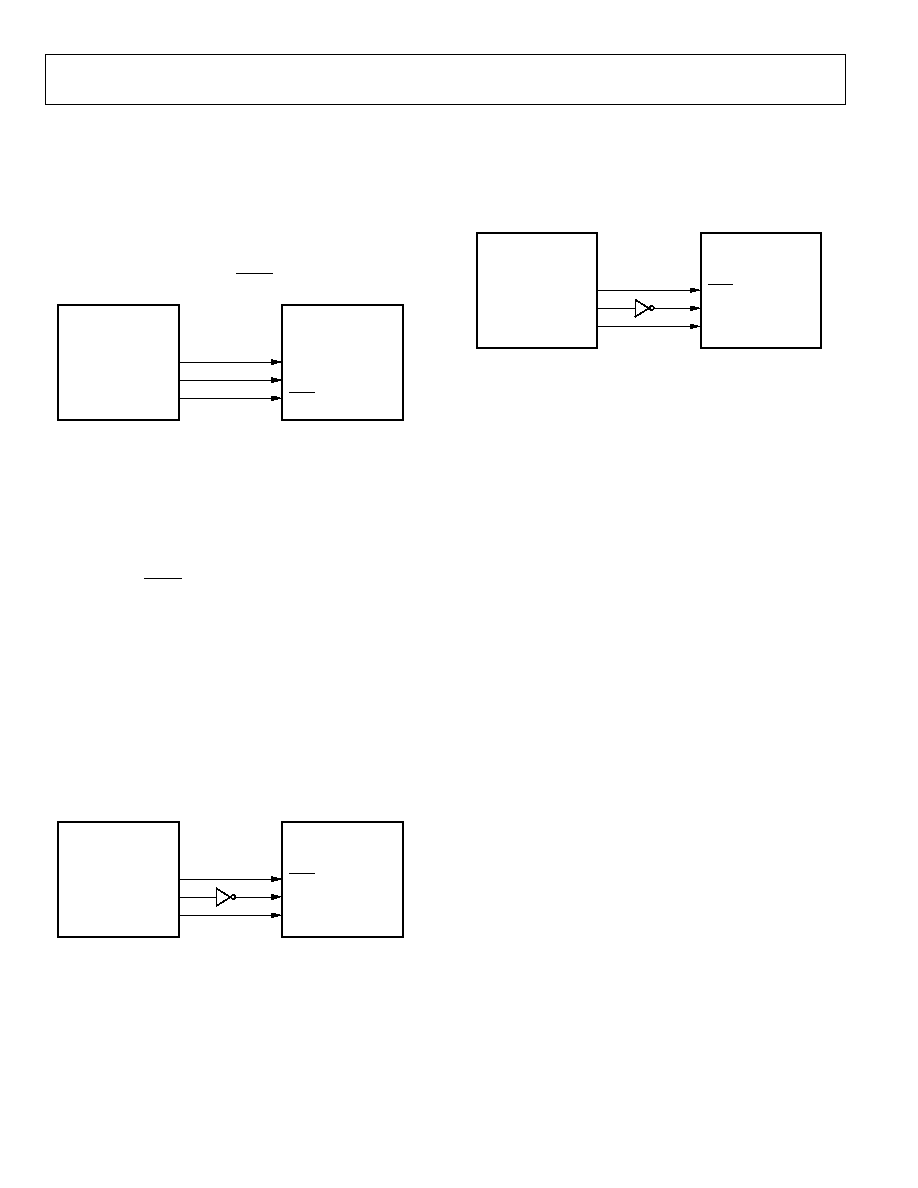
AD5040/AD5060 to ADSP-2101/ADSP-2103 Interface
Figure 45 shows a serial interface between the AD5040/AD5060
and the ADSP-2101/ADSP-2103. The ADSP-2101/ADSP-2103
should be set up to operate in the SPORT transmit alternate
framing mode. The ADSP-2101/ADSP-2103 sport is pro-
grammed through the SPORT control register and should be
configured for internal clock operation, active low framing, and
16-bit word length. Transmission is initiated by writing a word
to the Tx register after the SPORT has been enabled.
AD5040/
AD5060
1
1
ADDITIONAL PINS OMITTED FOR CLARITY
TFS
DT
SCLK
SYNC
DIN
SCLK
04767
-
030
ADSP-2101/
ADSP-2103
1
Figure 45. AD5040/AD5060 to ADSP-2101/ADSP-2103 Interface
AD5040/AD5060 to 68HC11/68L11 Interface
Figure 46 shows a serial interface between the AD5040/
AD5060 and the 68HC11/68L11 microcontroller. SCK of the
68HC11/68L11 drives the SCLK pin of the AD5040/AD5060,
while the MOSI output drives the serial data line of the DAC.
The SYNC signal is derived from a port line (PC7). The setup
conditions for correct operation of this interface require that the
68HC11/68L11 be configured so that its CPOL bit is 0 and its
CPHA bit is 1. When data is being transmitted to the DAC, the
SYNC line is taken low (PC7). When the 68HC11/68L11 is
configured where its CPOL bit is 0 and its CPHA bit is 1, data
appearing on the MOSI output is valid on the falling edge of
SCK. Serial data from the 68HC11/68L11 is transmitted in 8-bit
bytes with only 8 falling clock edges occurring in the transmit
cycle. Data is transmitted MSB first. In order to load data to the
AD5040/AD5060, PC7 is left low after the first eight bits are
transferred, and a second serial write operation is performed to
the DAC. PC7 is taken high at the end of this procedure.
AD5040/
AD5060
1
1
ADDITIONAL PINS OMITTED FOR CLARITY
PC7
SCK
MOSI
SYNC
SCLK
DIN
04767
-032
68HC11/
68L11
1
Figure 46. AD5040/AD5060 to 68HC11/68L11 Interface
AD5040/AD5060
Rev. 0 | Page 18 of 24
AD5040/AD5060 to Blackfin® ADSP-BF53x Interface
Figure 47 shows a serial interface between the AD5040/
AD5060 and the Blackfin ADSP-53x microprocessor. The
ADSP-BF53x processor family incorporates two dual-channel
synchronous serial ports, SPORT1 and SPORT0, for serial and
multiprocessor communications. Using SPORT0 to connect to
the AD5040/AD5060, the setup for the interface is: DT0PRI
drives the SDIN pin of the AD5040/AD5060, while TSCLK0
drives the SCLK of the part; the SYNC is driven from TFS0.
ADSP-BF53x
1
1
ADDITIONAL PINS OMITTED FOR CLARITY
DT0PRI
TSCLK0
TFS0
DIN
SCLK
SYNC
04767
-033
AD5040/
AD5060
1
Figure 47. AD5040/AD5060 to Blackfin® ADSP-BF53x Interface
AD5040/AD5060 to 80C51/80L51 Interface
Figure 48 shows a serial interface between the AD5060/
AD5040 and the 80C51/80L51 microcontroller. The setup
for the interface is: TxD of the 80C51/80L51 drives SCLK of
the AD5040/AD5060 while RxD drives the serial data line
of the part. The SYNC signal is again derived from a bit-
programmable pin on the port. In this case, Port Line P3.3 is
used. When data is to be transmitted to the AD5040, P3.3 is
taken low. The 80C51/80L51 transmits data only in 8-bit bytes;
thus only 8 falling clock edges occur in the transmit cycle. To
load data to the DAC, P3.3 is left low after the first eight bits are
transmitted, and a second write cycle is initiated to transmit the
second byte of data. P3.3 is taken high following the completion
of this cycle. The 80C51/80L51 outputs the serial data in a
format which has the LSB first. The AD5040/AD5060 require
data to be received with the MSB as the first bit. The
80C51/80L51 transmit routine should take this into account.
80C51/80L51
1
1
ADDITIONAL PINS OMITTED FOR CLARITY
P3.3
TxD
RxD
SYNC
SCLK
DIN
04767
-034
AD5040/
AD5060
1
Figure 48. AD5040/AD5060 to 80C51/80L51 Interface
AD5040/AD5060 to MICROWIRE Interface
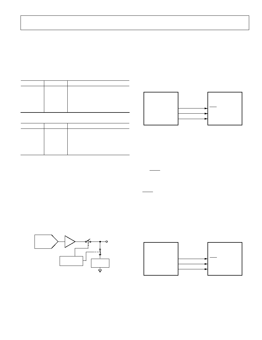
Figure 49 shows an interface between the AD5040/AD5060 and
any MICROWIRE-compatible device. Serial data is shifted out
on the falling edge of the serial clock and is clocked into the
AD5040/AD5060 on the rising edge of the SK.
MICROWIRE
1
1
ADDITIONAL PINS OMITTED FOR CLARITY
CS
SK
SO
SYNC
SCLK
DIN
04767
-035
AD5040/
AD5060
1
Figure 49. AD5040/AD5060 to MICROWIRE Interface
AD5040/AD5060
Rev. 0 | Page 19 of 24
APPLICATIONS
CHOOSING A REFERENCE FOR THE AD5040/
AD5060
To achieve the optimum performance from the AD5040/
AD5060, carefully choose a precision voltage reference. The
AD5040/AD5060 have just one reference input, V
REF
. The
voltage on the reference input is used to supply the positive
input to the DAC. Therefore, any error in the reference is
reflected in the DAC.
There are four possible sources of error to consider when
choosing a voltage reference for high accuracy applications:
initial accuracy, ppm drift, long-term drift, and output voltage
noise. Initial accuracy on the output voltage of the DAC leads
to a full-scale error in the DAC. To minimize these errors, a
reference with high initial accuracy is preferred. Also, choosing
a reference with an output trim adjustment, such as an ADR43x
device, allows a system designer to trim out system errors by
setting a reference voltage to a voltage other than the nominal.
The trim adjustment can also be used at temperature to trim
out any errors.
Because the supply current required by the AD5040/AD5060 is
extremely low, the parts are ideal for low supply applications.
The ADR395 voltage reference is recommended. This requires
less than 100 A of quiescent current and can, therefore, drive
multiple DACs in one system, if required. It also provides very
good noise performance at 8 V p-p in the 0.1 Hz to 10 Hz range.
SYNC
SCLK
DIN
7V
5V
V
OUT
= 0V TO 5V
ADR395
04767
-036
3-WIRE
SERIAL
INTERFACE
AD5040/
AD5060
Figure 50. ADR395 as Reference to AD5060/AD5040
Long-term drift is a measure of how much the reference drifts
over time. A reference with a tight long-term drift specification
ensures that the overall solution remains relatively stable during
its entire lifetime. The temperature coefficient of a reference
output voltage affects INL, DNL, and TUE. A reference with a
tight temperature coefficient specification should be chosen to
reduce the temperature dependence of the DAC output voltage
on ambient conditions.
In high accuracy applications, which have a relatively low noise
budget, reference output voltage noise needs to be considered. It
is important to choose a reference with as low an output noise
voltage as practical for the system noise resolution required.
Precision voltage references, such as the ADR435, produce low
output noise in the 0.1 Hz to 10 Hz region. Table 8 shows
examples of recommended precision references for use as a
supply to the AD5040/AD5060.
Table 8. Precision References for the AD5040/AD5060
Part No.
Initial
Accuracy
(mV max)
Temp. Drift
(ppm/°C max)
0.1 Hz to 10 Hz
Noise (V p-p typ)
ADR435 ±2
3
(SO-8)
8
ADR425
±2
3 (SO-8)
3.4
ADR02 ±3
3
(SO-8)
10
ADR02 ±3
3
(SC70)
10
ADR395 ±5
9
(TSOT-23)
8
BIPOLAR OPERATION USING THE AD5040/
AD5060
The AD5040/AD5060 have been designed for single-supply
operation, but a bipolar output range is also possible using the
circuit in Figure 51. The circuit shown yields an output voltage
range of ±5 V. Rail-to-rail operation at the amplifier output is
achievable using an AD8675/AD820/AD8032 or an OP196/
OP295.
The output voltage for any input code can be calculated as
×
-
+
×
×
=
1
R
2
R
V
1
R
2
R
1
R
D
V
V
DD
DD
O
65536
where D represents the input code in decimal (0 to 65536,
AD5060).
With V
REF
= 5 V, R1 = R2 = 10 k:
V
5
65536
10
-
×
=
D
V
O
Using the AD5060, this is an output voltage range of ±5 V
with 0x0000 corresponding to a -5 V output and 0xFFFF
corresponding to a +5 V output .
+5V
10
F
04767-037
R1 = 10k
V
OUT
V
REF
0.1
F
3-WIRE
SERIAL
INTERFACE
AD820/
OP295
+
5V
+5V
R2 = 10k
±5V
AD5040/
AD5060
Figure 51. Bipolar Operation with the AD5040/AD5060
AD5040/AD5060
Rev. 0 | Page 20 of 24
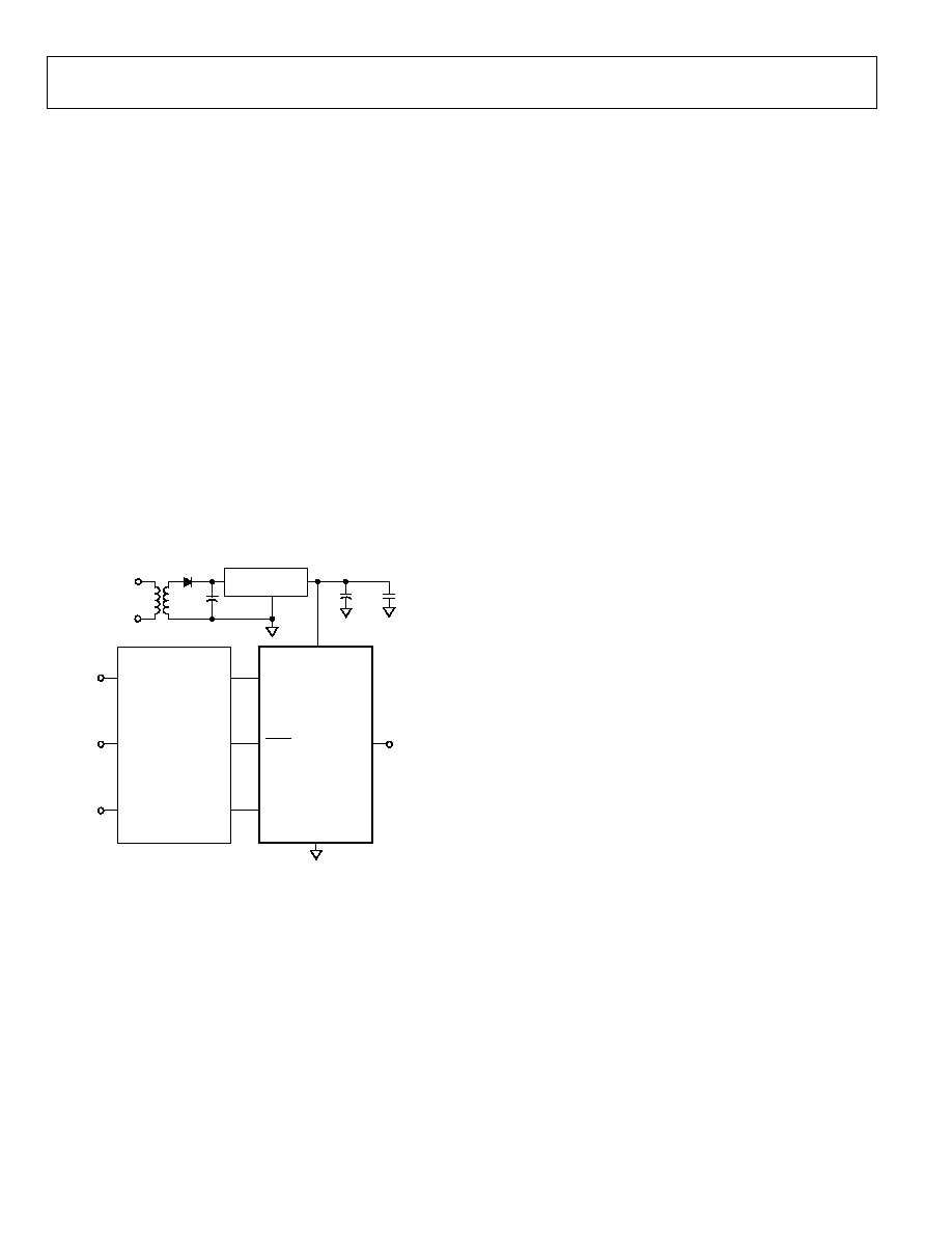
USING THE AD5040/AD5060 WITH A
GALVANICALLY ISOLATED INTERFACE CHIP
In process control applications in industrial environments, it is
often necessary to use a galvanically isolated interface to protect
and isolate the controlling circuitry from any hazardous
common-mode voltages that can occur in the area where the
DAC is functioning. iCoupler® provides isolation in excess of
2.5 kV. Because the AD5040/AD5060 use a 3-wire serial logic
interface, the ADuM130x family provides an ideal digital
solution for the DAC interface.
The ADuM130x isolators provide three independent isolation
channels in a variety of channel configurations and data rates.
They operate across the full range from 2.7 V to 5.5 V, providing
compatibility with lower voltage systems as well as enabling a
voltage translation functionality across the isolation barrier.
Figure 52 shows a typical galvanically isolated configuration
using the AD5040/AD5060. The power supply to the part
also needs to be isolated; this is accomplished by using a
transformer. On the DAC side of the transformer, a 5 V
regulator provides the 5 V supply required for the
AD5040/AD5060.
0.1
F
10
F
V
DD
GND
POWER
5V
REGULATOR
04767
-038
ADuM1300
SCLK
V0A
V1A
SCLK
V
OUT
SYNC
V0B
V1B
SDI
DIN
V0C
V1C
DATA
AD5040/
AD5060
Figure 52. AD5040/AD5060 with a Galvanically Isolated Interface
POWER SUPPLY BYPASSING AND GROUNDING
When accuracy is important in a circuit, it is helpful to carefully
consider the power supply and ground return layout on the
board. The printed circuit board containing the AD5040/
AD5060 should have separate analog and digital sections, each
having its own area of the board. If the AD5040/AD5060 are in
a system where other devices require an AGND-to-DGND
connection, the connection should be made at one point only.
This ground point should be as close as possible to the
AD5040/AD5060.
The power supply to the AD5040/AD5060 should be bypassed
with 10 F and 0.1 F capacitors. The capacitors should be
physically as close as possible to the device with the 0.1 F
capacitor ideally right up against the device. The 10 F
capacitors are the tantalum bead type. It is important that the
0.1 F capacitor has low effective series resistance (ESR) and
effective series inductance (ESI), as do common ceramic types
of capacitors. This 0.1 F capacitor provides a low impedance
path to ground for high frequencies caused by transient
currents due to internal logic switching.
The power supply line itself should have as large a trace as
possible to provide a low impedance path and reduce glitch
effects on the supply line. Clocks and other fast switching
digital signals should be shielded from other parts of the board
by a digital ground. Avoid crossover of digital and analog
signals, if possible. When traces cross on opposite sides of the
board, ensure that they run at right angles to each other to
reduce feedthrough effects on the board. The best board layout
technique is the microstrip technique where the component
side of the board is dedicated to the ground plane only, and the
signal traces are placed on the solder side. However, this is not
always possible with a two-layer board.
AD5040/AD5060
Rev. 0 | Page 21 of 24
OUTLINE DIMENSIONS
1
3
5
6
2
8
4
7
2.90 BSC
1.60 BSC
1.95
BSC
0.65 BSC
0.38
0.22
0.15 MAX
1.30
1.15
0.90
SEATING
PLANE
1.45 MAX
0.22
0.08
0.60
0.45
0.30
8°
4°
0°
2.80 BSC
PIN 1
INDICATOR
COMPLIANT TO JEDEC STANDARDS MO-178-BA
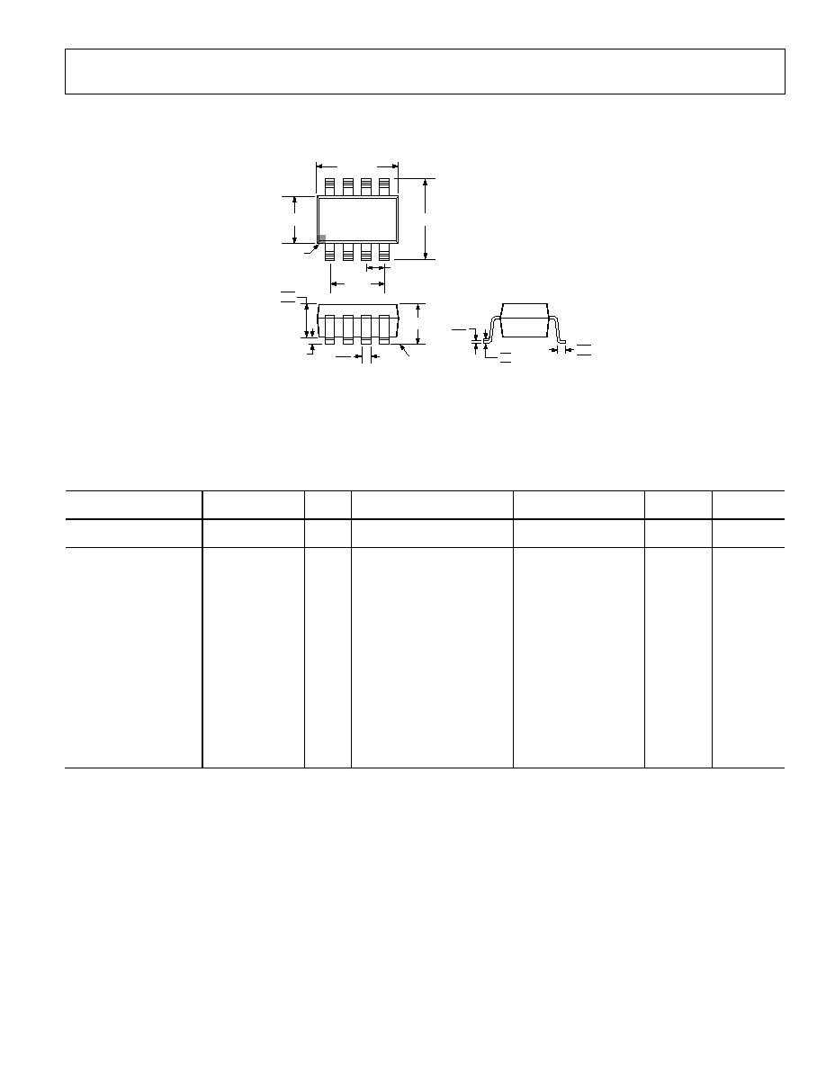
Figure 53. 8-Lead Small Outline Transistor Package [SOT-23]
(RJ-8)
Dimensions shown in millimeters
ORDERING GUIDE
Model
Temperature
Range INL
Description
Package
Description
Package
Option Branding
AD5040BRJZ-500RL7
1
-40°C to +85°C
1 LSB
2.7 V to 5.5 V, reset to 0 V
8 Lead SOT-23
RJ-8
D4C
AD5040BRJZ-REEL7
1
-40°C to +85°C
1 LSB
2.7 V to 5.5 V, reset to 0 V
8 Lead SOT-23
RJ-8
D4C
AD5060ARJZ-1500RL7
1
-40°C to +85°C
2 LSB
2.7 V to 5.5 V, reset to 0 V
8 Lead SOT-23
RJ-8
D3Z
AD5060ARJZ-1REEL7
1
-40°C to +85°C
2 LSB
2.7 V to 5.5 V, reset to 0 V
8 Lead SOT-23
RJ-8
D3Z
AD5060ARJZ-2REEL7
1
-40°C to +85°C
2 LSB
2.7 V to 5.5 V, reset to mid-
scale
8 Lead SOT-23
RJ-8
D41
AD5060ARJZ-2500RL7
1
-40°C to +85°C
2 LSB
2.7 V to 5.5 V, reset to mid-
scale
8 Lead SOT-23
RJ-8
D41
AD5060BRJZ-1500RL7
1
-40°C to +85°C
1 LSB
2.7 V to 5.5 V, reset to 0 V
8 Lead SOT-23
RJ-8
D3W
AD5060BRJZ-1REEL7
1
-40°C to +85°C
1 LSB
2.7 V to 5.5 V, reset to 0 V
8 Lead SOT-23
RJ-8
D3W
AD5060BRJZ-2REEL7
1
-40°C to +85°C
1 LSB
2.7 V to 5.5 V, reset to mid-
scale
8 Lead SOT-23
RJ-8
D3X
AD5060BRJZ-2500RL7
1
-40°C to +85°C
1 LSB
2.7 V to 5.5 V, reset to mid-
scale
8 Lead SOT-23
RJ-8
D3X
AD5060YRJZ-1500RL7
1
-40°C to +125°C
1 LSB
2.7 V to 5.5 V, reset to 0 V
8 Lead SOT-23
RJ-8
D6F
AD5060YRJZ-1REEL7
1
-40°C to +125°C
1 LSB
2.7 V to 5.5 V, reset to 0 V
8 Lead SOT-23
RJ-8
D6F
EVAL-AD5060EB
Evaluation
Board
EVAL-AD5040EB
Evaluation
Board
1
Z = Pb-free part.

AD5040/AD5060
Rev. 0 | Page 22 of 24
NOTES

AD5040/AD5060
Rev. 0 | Page 23 of 24
NOTES

AD5040/AD5060
Rev. 0 | Page 24 of 24
T
NOTES
© 2005 Analog Devices, Inc. All rights reserved. Trademarks and
registered trademarks are the property of their respective owners.
D04767010/05(0)
TTT
Document Outline
- þÿ
- þÿ
- þÿ
- FUNCTIONAL BLOCK DIAGRAM
- þÿ
- þÿ
- þÿ
- þÿ
- þÿ
- þÿ
- þÿ
- þÿ
- þÿ
- þÿ
- SERIAL INTERFACE
- POWER-ON RESET
- þÿ
- POWER-DOWN MODES
- þÿ
- þÿ
- þÿ
- þÿ
- þÿ
- POWER SUPPLY BYPASSING AND GROUNDING
- þÿ