 | –≠–ª–µ–∫—Ç—Ä–æ–Ω–Ω—ã–π –∫–æ–º–ø–æ–Ω–µ–Ω—Ç: AAT7202 | –°–∫–∞—á–∞—Ç—å:  PDF PDF  ZIP ZIP |

Advanced Analog Technology, Inc.
≠
≠
Advanced Analog Technology, Inc
. V 0.1
AAT7202
Preliminary AAT7202
12+1-Channel Buffer for TFT LCD
Features
12 Channels with Output Current: +30mA
(MAX)
1 Vcom with Output Current:
+100mA
(MAX)
Unity Gain Buffer Capable of Driving
Large Capacitive Loads
Input range Matched to LCD Reference
Requirements
Specified for -20
o
C to +85
o
C...6.5V to
16V
TQFP-48 Pins
General Description
The AAT7200 consists of 12+1 channel
buffers target toward the needs of thin film
transistor liquid crystal display (TFT LCD).
This device consist of a Vcom buffer circuits,
four rail to rail buffer amplifiers circuits and
8 buffer amplifiers circuits. Each buffer is
capable of driving heavy capacitive loads and
offers fast load current (Vcom : 100mA, the
others : 30mA).
.
Pin Configuration
TOP VIEW

Advanced Analog Technology, Inc.
≠
≠
Advanced Analog Technology, Inc
. V 0.1
AAT7202
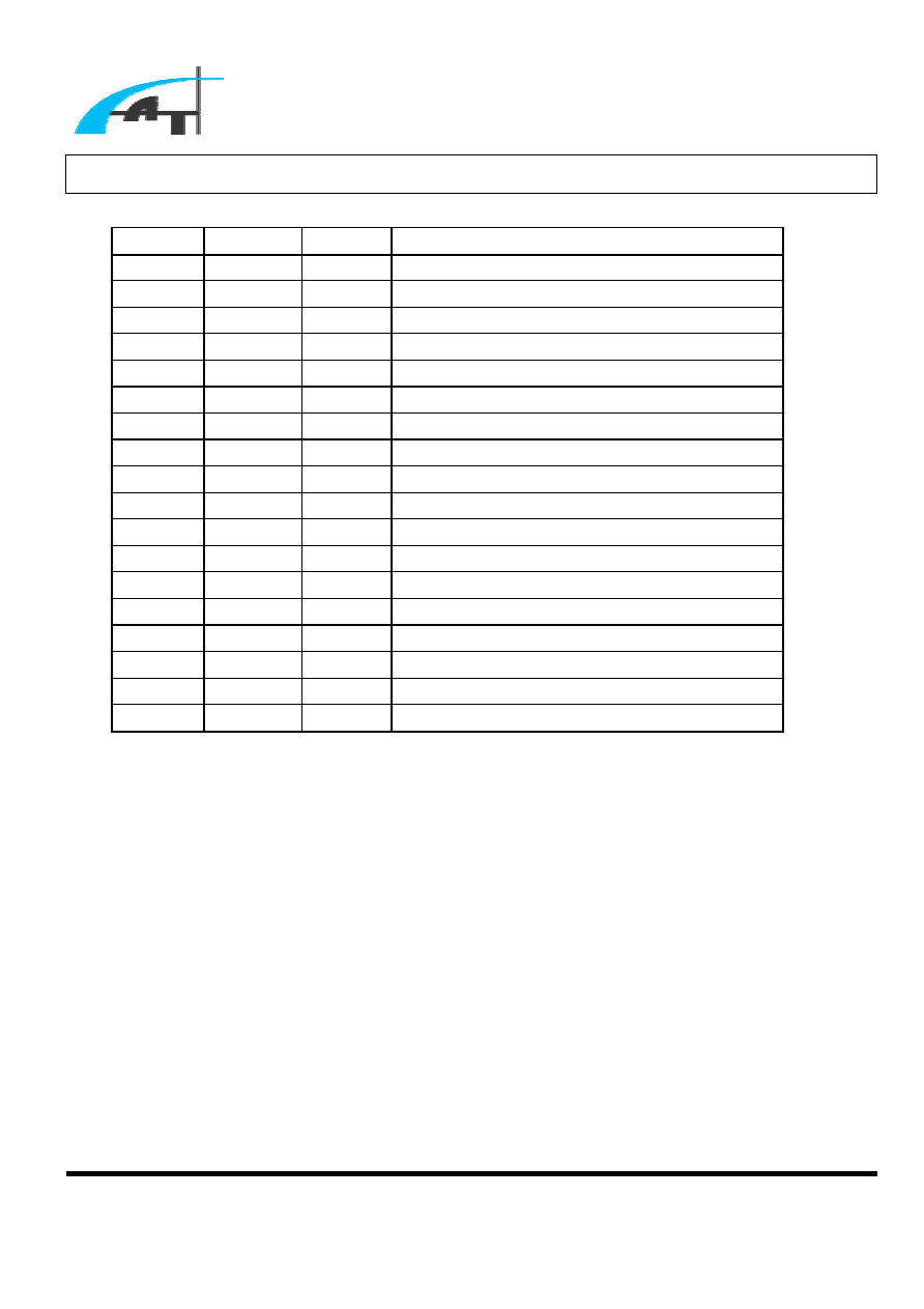
Pin Description
Pin #
Name
I/O
Description
1
o11
O
Buffer Channel 11 Output
2
o10
O
Buffer Channel 10 Output
3
o9
O
Buffer Channel 9 Output
4
o8
O
Buffer Channel 8 Output
5
o7
O
Buffer Channel 7 Output
6 N.C.
7 VSS I
Ground
8 VDD I
Power
9 N.C.
10
o6
O
Buffer Channel 6 Output
11
o5
O
Buffer Channel 5 Output
12
o4
O
Buffer Channel 4 Output
13
o3
O
Buffer Channel 3 Output
14 N.C.
15 VDD I
Power
16 N.C.
17 N.C.
18 o2 O
Buffer Channel 2 Output
19 VSS I
Ground
20
o1
O
Buffer Channel 1 Output
21 VSS I
Ground
22 VDD I
Power
23
i1
I
Buffer Channel 1 Input
24
i2
I
Buffer Channel 2 Input
25
i3
I
Buffer Channel 3 Input
26
i4
I
Buffer Channel 4 Input
27 i5 I
Buffer Channel 5 Input
28
i6
I
Buffer Channel 6 Input
29 N.C.
30 VDD I
Power
*
To be continued
Advanced Analog Technology, Inc.
≠
≠
Advanced Analog Technology, Inc
. V 0.1
AAT7202
Pin #
Name
I/O
Description
31 VSS I
Ground
32 N.C.
33
i7
I
Buffer Channel 7 Input
34
i8
I
Buffer Channel 8 Input
35
i9
I
Buffer Channel 9 Input
36
i10
I
Buffer Channel 10 Input
37
i11
I
Buffer Channel 11 Input
38
i12
I
Buffer Channel 12 Input
39
Icom
I
Com Buffer Input
40 N.C.
41 N.C.
42 N.C.
43 VDD
I
Power
44 VSS I
Ground
45 VDD
I
Power
46 VSS I
Ground
47 Ocom
O
Com
Buffer Output
48
o12
O
Buffer Channel 12 Output

Advanced Analog Technology, Inc.
≠
≠
Advanced Analog Technology, Inc
. V 0.1
AAT7202
Absolute Maximum Ratings
CHARACTERISTICS SYMBOL VALUE UNIT
Supply voltage
V
DD
+18
V
Input Voltage
V
I
5
.
0
-
to
5
.
0
V
DD
+
V
Maximum Junction Temperature
T
J
+125
o
C
Operating Temperature
T
ope
-40 to +85
o
C
Storage Temperature
T
stg
-65 to 150
o
C
Lead Temperature(Soldering,10 second)
---
260
o
C
Note1:
Value beyond absolute maximum ratings may cause permanent damage to the device.

Advanced Analog Technology, Inc.
≠
≠
Advanced Analog Technology, Inc
. V 0.1
AAT7202
Electrical Characteristics
(V
DD
=10V, T
A
=25
o
C unless otherwise specified.)
Power Supply Performance
Parameter
Test
Conditions Min
Typ
Max
Units
Power Supply Rejection
Ratio[2]
PSRR
V
DD
is moved from 6.5V to
15.5V
80 dB
Supply Current
I
S
9 mA
Input Characteristics
Parameter
Test
Conditions Min
Typ
Max
Units
Input Offset Voltage
V
OS
Vin=VDD/2 , Vout =VDD/2
2
12
mV
Input Bias Current
I
B
Vin=VDD/2 , Vout =VDD/2
2
50
nA
Output Characteristics
Parameter
Test
Conditions Min
Typ
Max
Units
I
L
=5mA(Buffer 1,2,11,12)
Vin=0v
0.08
0.15
V
Output Swing Low
V
OL
I
L
=10mA (Buffer 3,4,...,9,10)
Vin=1v
1.02 1.05
V
I
L
=-5mA (Buffer 1,2,11,12)
Vin=10v
9.85 9.92
V
Output Swing High
V
OH
I
L
=-10mA (Buffer 3,4,...,9,10)
Vin=9v
8.95 8.98
V
V
OL
I
L
=10mA Vin=5v
5.02
5.04
V
Output Swing
(buffer 3,4,...,9,10)
V
OH
I
L
=-10mA Vin=5v
4.96
4.98
V
V
OL
I
L
=50mA Vin=5v
5.03
5.05
V
Output Swing
(COM)
V
OH
I
L
=-50mA Vin=5v
4.95
4.97
V
(Buffer 1~12 )
+70
mA
Short Circuit Current
I
SC
(Com Buffer)
+180
mA