
Advanced Power
N-CHANNEL ENHANCEMENT MODE
Electronics Corp.
POWER MOSFET
Dynamic dv/dt Rating
BV
DSS
600/650/700V
Repetitive Avalanche Rated
R
DS(ON)
2.4
Fast Switching
I
D
4A
Simple Drive Requirement
Description
Absolute Maximum Ratings
Symbol
Units
V
DS
Drain-Source Voltage
V
V
GS
Gate-Source Voltage
V
I
D
@T
C
=25
Continuous Drain Current, V
GS
@ 10V
A
I
D
@T
C
=100
Continuous Drain Current, V
GS
@ 10V
A
I
DM
Pulsed Drain Current
1
A
P
D
@T
C
=25
Total Power Dissipation
W
W/
E
AS
Single Pulse Avalanche Energy
2
mJ
I
AR
Avalanche Current
A
E
AR
Repetitive Avalanche Energy
mJ
T
STG
T
J
Operating Junction Temperature Range
Thermal Data
Symbol
Value
Unit
Rthj-c
Thermal Resistance Junction-case
Max.
2.0
/W
Rthj-a
Thermal Resistance Junction-ambient
Max.
62
/W
Data & specifications subject to change without notice
20030332
AP04N70BP
100
-55 to 150
Parameter
4
4
Parameter
Rating
600/650/700
- /A/H
4
2.5
Storage Temperature Range
-55 to 150
15
62.5
Linear Derating Factor
0.5
AP04N70 series are specially designed as main switching devices for
universal 90~265VAC off-line AC/DC converter applications. TO-220
type provide high blocking voltage to overcome voltage surge and sag in
the toughest power system with the best combination of fast
switching,ruggedized design and cost-effectiveness.
The TO-220 package is universally preferred for all commercial-
industrial applications. The device is suited for switch mode power
supplies ,DC-AC converters and high current high speed switching
circuits.
� 3
0
G
D
S
G
D
S
TO-220

Electrical Characteristics@T
j
=25
o
C(unless otherwise specified)
Symbol
Parameter
Test Conditions
Min.
Typ. Max. Units
BV
DSS
Drain-Source Breakdown Voltage
V
GS
=0V, I
D
=1mA / -
600
-
-
V
V
GS
=0V, I
D
=1mA / A
650
-
-
V
V
GS
=0V, I
D
=1mA / H
700
-
-
V
B
V
DSS
/T
j
Breakdown Voltage Temperature Coefficient
Reference to 25
, I
D
=1mA
-
0.6
-
V/
R
DS(ON)
Static Drain-Source On-Resistance
V
GS
=10V, I
D
=2A
-
-
2.4
V
GS(th)
Gate Threshold Voltage
V
DS
=V
GS
, I
D
=250uA
2
-
4
V
g
fs
Forward Transconductance
V
DS
=10V, I
D
=2A
-
2.5
-
S
I
DSS
Drain-Source Leakage Current (T
j
=25
o
C)
V
DS
=600V, V
GS
=0V
-
-
10
uA
Drain-Source Leakage Current (T
j
=150
o
C)
V
DS
=480V
,
V
GS
=0V
-
-
100
uA
I
GSS
Gate-Source Leakage
V
GS
=
-
-
nA
Q
g
Total Gate Charge
3
I
D
=4A
-
16.7
-
nC
Q
gs
Gate-Source Charge
V
DS
=480V
-
4.1
-
nC
Q
gd
Gate-Drain ("Miller") Charge
V
GS
=10V
-
4.9
-
nC
t
d(on)
Turn-on Delay Time
3
V
DD
=300V
-
11
-
ns
t
r
Rise Time
I
D
=4A
-
8.3
-
ns
t
d(off)
Turn-off Delay Time
R
G
=10
,
V
GS
=10V
-
23.8
-
ns
t
f
Fall Time
R
D
=75
-
8.2
-
ns
C
iss
Input Capacitance
V
GS
=0V
-
950
-
pF
C
oss
Output Capacitance
V
DS
=25V
-
65
-
pF
C
rss
Reverse Transfer Capacitance
f=1.0MHz
-
6
-
pF
Source-Drain Diode
Symbol
Parameter
Test Conditions
Min.
Typ. Max. Units
I
S
Continuous Source Current ( Body Diode )
V
D
=V
G
=0V , V
S
=1.5V
-
-
4
A
I
SM
Pulsed Source Current ( Body Diode )
1
-
-
15
A
V
SD
Forward On Voltage
3
T
j
=25
, I
S
=4A, V
GS
=0V
-
-
1.5
V
Notes:
1.Pulse width limited by safe operating area.
2.Starting Tj=25
o
C , V
DD
=50V , L=25mH , R
G
=25
, I
AS
=4A.
3.Pulse width <300us , duty cycle <2%.
Ordering Code
AP04N70BP- X : X Denote BV
DSS
Grade
Blank = BV
DSS
600V
A
= BV
DSS
650V
H
= BV
DSS
700V
AP04N70BP
�
100
�
30V

Fig 1. Typical Output Characteristics
Fig 2. Typical Output Characteristics
Fig 3. Normalized BV
DSS
v.s. Junction
Fig 4. Normalized On-Resistance
Temperature
v.s. Junction Temperature
AP04N70BP
0.8
0.9
1
1.1
1.2
-50
0
50
100
150
T
j
, Junction Temperature (
o
C)
No
rm
a
lize
d
BV
DS
S
(V)
0
0.5
1
1.5
2
2.5
-50
0
50
100
150
T
j
, Junction Temperature (
o
C )
No
rm
a
lize
d
R
DS
(ON)
V
G
=10V
I
D
=2A
0
0.5
1
1.5
2
2.5
0
1
2
3
4
5
6
7
V
DS
, Drain-to-Source Voltage (V)
I
D
,
Dra
i
n C
u
rre
nt
(A
)
T
C
=25
o
C
V
G
=10V
V
G
=6.0V
V
G
=5.0V
V
G
=4.5V
V
G
=4.0V
0
0.5
1
1.5
2
0
2
4
6
8
10
12
V
DS
, Drain-to-Source Voltage (V)
I
D
,
Dra
i
n C
u
rre
nt
(A
)
T
C
=150
o
C
V
G
=4.0V
V
G
=3.5V
V
G
=4.5V
V
G
=5.0V
V
G
=6.0V
V
G
=10V
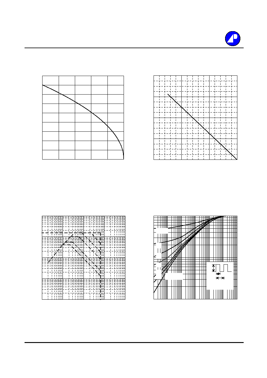
Fig 5. Maximum Drain Current v.s.
Fig 6. Typical Power Dissipation
Case Temperature
Fig 7. Maximum Safe Operating Area
Fig 8. Effective Transient Thermal Impedance
AP04N70BP
0
20
40
60
80
0
50
100
150
T
c ,
Case Temperature (
o
C )
P
D
(W
)
0
0.5
1
1.5
2
2.5
3
3.5
4
4.5
25
50
75
100
125
150
T
c
, Case Temperature (
o
C )
I
D
,
Dra
i
n C
u
rre
nt
(A
)
0.01
0.1
1
10
100
1
10
100
1000
10000
V
DS
(V)
I
D
(A)
T
c
=25
o
C
Single Pulse
10us
100us
1ms
10ms
100ms
0.01
0.1
1
0.00001
0.0001
0.001
0.01
0.1
1
10
t , Pulse Width (s)
N
o
r
m
aliz
ed T
h
er
m
a
l Res
pon
s
e
(
R
th
jc
)
P
DM
Duty factor = t/T
Peak T
j
= P
DM
x R
thjc
+ T
C
t
T
0.02
0.01
0.05
0.1
0.2
DUTY=0.5
SINGLE PULSE

Fig 9. Gate Charge Characteristics
Fig 10. Typical Capacitance Characteristics
Fig 11. Forward Characteristic of
Fig 12. Gate Threshold Voltage v.s.
Reverse Diode
Junction Temperature
AP04N70BP
0
1
2
3
4
5
-50
0
50
100
150
T
j
, Junction Temperature (
o
C )
V
GS
(t
h
)
(V)
0.1
1
10
100
0
0.2
0.4
0.6
0.8
1
1.2
1.4
1.6
V
SD
(V)
I
S
(A)
T
j
= 25
o
C
T
j
=150
o
C
1
100
10000
1
6
11
16
21
26
31
V
DS
(V)
C (
p
F)
f=1.0MHz
Ciss
Coss
Crss
0
2
4
6
8
10
12
14
16
0
5
10
15
20
25
Q
G
, Total Gate Charge (nC)
V
GS
, G
a
te to S
o
u
r
ce Voltage (
V
)
I
D
=4A
V
DS
=320V
V
DS
=400V
V
DS
=480V